Embedded system and page relocation method therefor

a page relocation and embedded system technology, applied in the direction of memory address formation, memory address allocation/allocation/relocation, instruments, etc., can solve the problems of reducing affecting the efficiency of memory management, so as to reduce power consumption and reduce leakage current , the effect of maximizing the number of memory banks

Active Publication Date: 2011-03-01
ELECTRONICS & TELECOMM RES INST
View PDF12 Cites 2 Cited by
  • Summary
  • Abstract
  • Description
  • Claims
  • Application Information

AI Technical Summary

Benefits of technology

[0011]An embodiment of the present invention is directed to providing an embedded system for minimizing leakage current generated in a memory and a method for relocating pages therefor.
[0017]The development of a deep-submicron semiconductor technology enables to form gate oxide thinner than 90 nm. Therefore, a leakage current that is generated at below a threshold voltage is equivalent to almost of all power consumption of entire system. Particularly, the leakage current of a memory area is a critical part of overall power consumption because the number of gates in a memory abruptly increases compared to the number of all gates in an embedded system having a processor and a memory. In the present invention, a memory is divided into a plurality of memory banks, and a circuit for cutting off the leakage current of each memory banks is included. Then, the power consumption is reduced by dynamically cutting off the leakage current of memory banks that are not in use while the system is operating. Particularly, a leakage current is dynamically controlled by relocating data used by a processor using a data relocating circuit.
[0018]In the present embodiment, a memory is divided into a plurality of physical memory banks. In a view of a processor, a memory is divided into a plurality of logical memory pages, and a data relocating circuit decides a memory bank where each of memory pages is physically located. The processor accesses a physical memory bank with reference to a data relocating circuit when the processor reads data from the memory. Initially, all memory banks are inactivated (turn-off) to remove the leakage current. If a processor requests to store data in a memory, the data relocating circuit activates (turn-on) a corresponding memory bank. The processor requests memory bank invalidation when all memory pages in the memory bank are not valid any more. If the memory bank is invalidated by the processor, all memory pages in the memory bank are invalidated. The inactivated memory bank is cut off with power, thereby reducing leakage current. The data relocating circuit according to the present invention maximizes the number of memory banks with the power cut off while the processor is operating, thereby minimizing the leakage current.

Problems solved by technology

Since the flow of charge is current, it is the major factor of the power consumption.
Meanwhile, further the semiconductor manufacturing process is advanced, more the leakage power occurs.
Since thin gate oxide cannot stand high voltage, it is required to lower the operating voltage of a semiconductor circuit.
However, these methods cannot reduce the leakage current.
In case of a Flip-flop or a memory, memorized data is lost if the power is cut off.
However, it is very rare to operate the entire embedded system in the power down mode.

Method used


Image

  • Embedded system and page relocation method therefor
  • Embedded system and page relocation method therefor
  • Embedded system and page relocation method therefor

Examples


Embodiment Construction

[0022]The advantages, features and aspects of the invention will become apparent from the following description of the embodiments with reference to the accompanying drawings, which is set forth hereinafter.

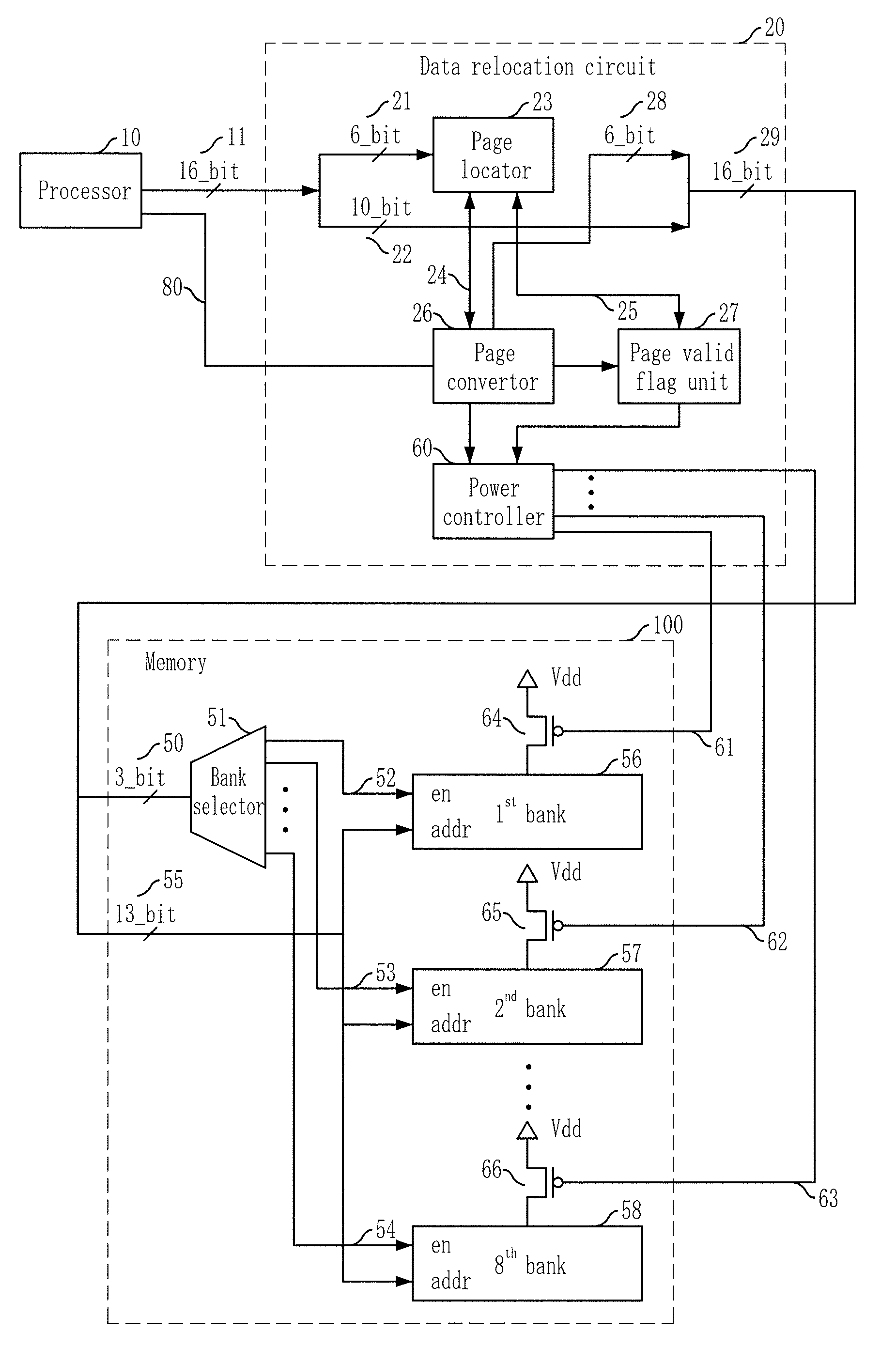
[0023]FIG. 1 is a block diagram illustrating an embedded system in accordance with an embodiment of the present invention.

[0024]Referring to FIG. 1, the embedded system according to the present embodiment includes a processor 10, a data relocating circuit 20, and a memory 100.

[0025]The processor 10, for example, a digital signal processor (DSP) Core, performs a read operation or a write operation to read or write data on the memory at every clock cycle. Particularly, a digital signaling processor (DSP) simultaneously performs a plurality of read and write operations to read or write server data at every clock cycles. As shown in FIG. 1, the embedded system 10 according to the present embodiment outputs 16-bits of a logical memory address 11. The logical memory address 11 inputs t...


PUM


Abstract

Provided are an embedded system and a method for relocating memory pages therefor. The embedded system includes a processor, a data relocating circuit for receiving a logical address from the processor, mapping the received logical address to a physical address to locate a valid page in a predetermined bank, and generating a bank power control signal according to whether or not a corresponding memory bank includes valid pages, and a memory including a plurality of memory banks addressed by a physical address outputted from the data relocating circuit and a plurality of switching means for selectively supplying a power voltage to each of memory banks in response to the bank power control signal.

Description

CROSS-REFERENCES TO RELATED APPLICATIONS[0001]The present invention claims priority of Korean Patent Application Nos. 10-2006-0122489 and 10-2007-0106829, filed on Dec. 5, 2006, and Oct. 23, 2007, respectively, which are incorporated herein by reference.BACKGROUND OF THE INVENTION[0002]1. Field of the Invention[0003]The present invention relates to a semiconductor design technology and, more particularly, to an embedded system having a processor and a memory and a method for relocating memory pages in the embedded system.[0004]This work was supported by the Information Technology (IT) research and development program of the Korean Ministry of Information and Communication (MIC) and / or the Korean Institute for Information Technology Advancement (IITA) [2006-S-048-01, “embedded DSP platform for processing audio and video signal”].[0005]2. Description of Related Art[0006]The development of an information technology (IT) makes portable devices popular. Various types of portable devices ...

Claims


Application Information

Patent Timeline
Patent Type & Authority Patents(United States)
IPC IPC(8): G06F12/00
CPCG06F1/3225G06F1/3275G06F1/3287G06F12/0292G06F12/06Y02B60/1228Y02B60/1282G06F12/023Y02D10/00
Inventor KWON, YOUNG-SUKOO, BON-TAEEUM, NAK-WOONG
Owner ELECTRONICS & TELECOMM RES INST
Why Eureka
Try Eureka