Image sensor having heterojunction bipolar transistor and method of fabricating the same

a technology of image sensor and heterojunction bipolar transistor, which is applied in the direction of electrical equipment, semiconductor devices, radio frequency controlled devices, etc., can solve the problems of difficult to make the ccd image sensor highly integrated, the fabrication of the ccd image sensor is incompatible with that of the typical cmos device, and the nanoscale cmos circuit cannot be easily applied, etc., to achieve excellent three-color balance characteristics

Inactive Publication Date: 2011-03-08
ELECTRONICS & TELECOMM RES INST
View PDF23 Cites 9 Cited by
  • Summary
  • Abstract
  • Description
  • Claims
  • Application Information

AI Technical Summary

Benefits of technology

[0016]Also, the present invention is directed to an image sensor and a method of fabricating the same capable of reducing the number of transistors in the pixel and preventing degradation of signals at low exposure.
[0018]In addition, the present invention is directed to an image sensor with an excellent three-color balance characteristic and a method of fabricating the same.

Problems solved by technology

However, since the CCD image sensor requires a high voltage of 10V or higher, a nanoscale CMOS circuit cannot be easily applied to the CCD image sensor, so it is difficult to make the CCD image sensor highly integrated.
Also, fabrication of the CCD image sensor is incompatible with that of typical CMOS devices.
Thus, an image sensor module is made bulky because it needs to include at least two chips.
Further, the CCD image sensor consumes at least ten times as much power as the CIS due to the high voltage, thus it is not suitable for portable data terminals.
However, the CIS is being fabricated using CMOS technology in the 180-nm regime, but fabrication of sub-90-nm nanoscale CISs has not yet been attained.
In contrast, a method using the reverse-operational bipolar transistor can amplify the optical signal on its own, but its gain characteristic is poor.

Method used


Image

  • Image sensor having heterojunction bipolar transistor and method of fabricating the same
  • Image sensor having heterojunction bipolar transistor and method of fabricating the same
  • Image sensor having heterojunction bipolar transistor and method of fabricating the same

Examples


embodiment

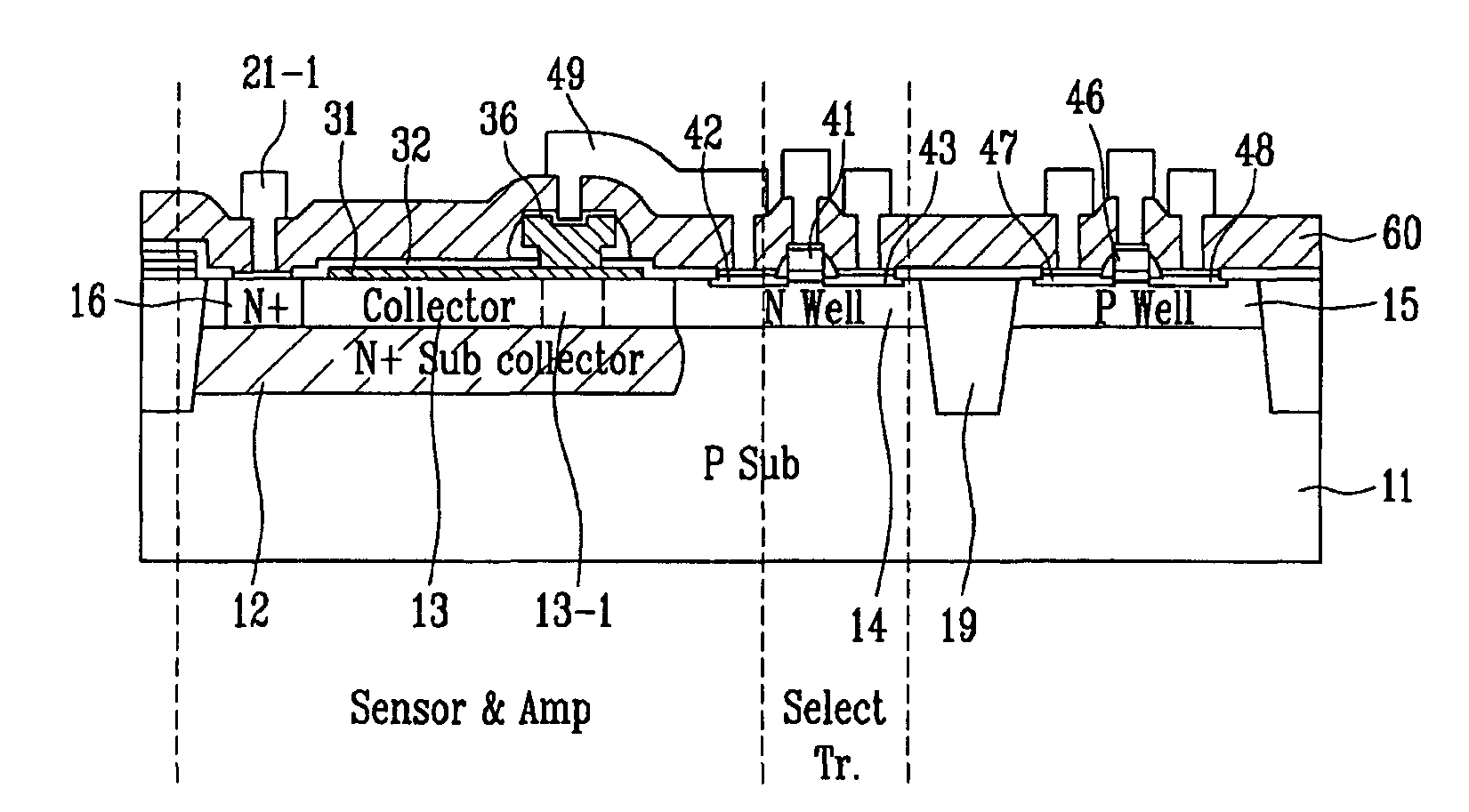
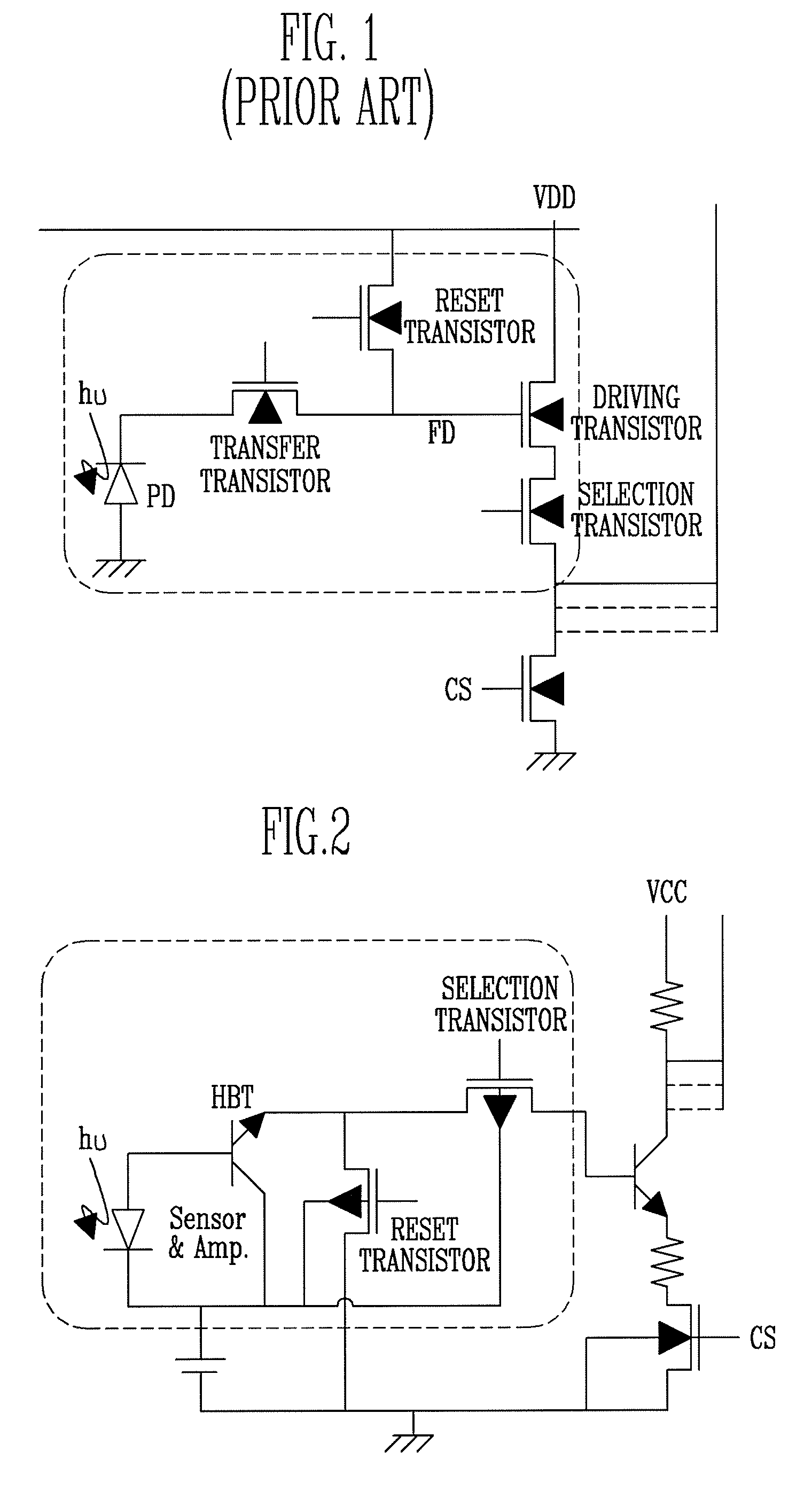
[0030]Referring to FIG. 2, an image sensor according to an exemplary embodiment of the present invention includes a photo diode (PD), a heterojunction bipolar transistor (HBT), a reset p-channel metal-oxide semiconductor (PMOS) transistor, and a line selection PMOS transistor. The PD has a cathode connected to a power supply voltage terminal. The HBT has a base connected to an anode of the PD, a collector connected to the cathode of the PD, and an emitter from which an amplified sensing signal is generated. The reset PMOS transistor serves to connect the emitter of the HBT with a ground voltage terminal in response to a reset signal applied to a gate. Also, the line selection PMOS transistor serves to externally transmit an emitter signal from the bipolar transistor in response to a line selection signal applied to the gate.

[0031]Noticeably, since it is desirable that the image sensor according to the present exemplary embodiment's fabrication should be based on SiGe BiCMOS technolo...


PUM


Abstract

Provided is an image sensor having a heterojunction bipolar transistor (HBT) and a method of fabricating the same. The image sensor is fabricated by SiGe BiCMOS technology. In the image sensor, a PD employs a floating-base-type SiGe HBT. A floating base of the SiGe HBT produces a positive voltage with respect to a collector during an exposure process, and the HBT performs a reverse bipolar operation due to the positive voltage so that the collector and an emitter exchange functions. The SiGe HBT can sense an optical current signal and also amplify the optical current signal. The image sensor requires only three transistors in a pixel so that the degree of integration can increase. The image sensor has an improved sensitivity of signals in the short wavelength region and a sensing signal has excellent linearity such that both a sensing mechanism and control circuit are very simple.

Description

CROSS-REFERENCE TO RELATED APPLICATION[0001]This application claims priority to and the benefit of Korean Patent Application No. 2006-0104170, filed Oct. 25, 2006, the disclosure of which is incorporated herein by reference in its entirety.BACKGROUND[0002]1. Field of the Invention[0003]The present invention relates to an image sensor having a heterojunction bipolar transistor (HBT) and, more specifically, to an image sensor in which a complementary metal oxide semiconductor (CMOS) device and a silicon-germanium HBT (SiGe HBT) are mounted on a substrate using SiGe bipolar junction transistor CMOS (SiGe BiCMOS) technology, and a method of fabricating the same.[0004]The image sensor according to the present invention can be more highly integrated than a conventional CMOS image sensor (CIS), and more highly sensitive to signals than when it is fabricated using typical bipolar technology because the amplification rate of signals becomes higher in a floating base reverse-operational mode....

Claims


Application Information

Patent Timeline
Patent Type & Authority Patents(United States)
IPC IPC(8): H01L31/11
CPCH01L27/14609H01L27/14681H01L27/14689H01L27/146H01L29/737
Inventor KANG, JIN YEONGLEE, SANG HEUNGKOO, JIN GUN
Owner ELECTRONICS & TELECOMM RES INST
Why Eureka
Try Eureka