Stamp for micro/nano imprint lithography using diamond-like carbon and method of fabricating the same

a technology of diamond-like carbon and imprint lithography, which is applied in the field of micro/nano imprint lithography and the method of fabricating the same, can solve the problems of difficult multi-alignment, break down of the structure made of heat curable materials, and difficulty in printing techniques using heat, so as to achieve the effect of improving hydrophobic properties and acquiring process stability

Active Publication Date: 2011-03-29
KOREA INST OF MACHINERY & MATERIALS
View PDF19 Cites 51 Cited by
  • Summary
  • Abstract
  • Description
  • Claims
  • Application Information

AI Technical Summary

Benefits of technology

[0036]As explained hereinabove, according to the method for fabricating a stamp for micro / nano imprint lithography of the present invention, the stamp is fabricated by patterning the diamond -like carbon thin film deposited on the substrate, the diamond-like carbon thin film which is hydrophobic and light-transmittable, especially ultraviolet ray-transmittable so that the sticking may be prevented at imprinting between the resist and the stamp without an anti-sticking layer.
[0037]Also, the problems caused by the previous anti-sticking layer may be prevented so that a wanted pattern may be obtained and the process stability may be acquired.
[0038]In addition, the hydrophobic property may be improved by pouring a fluorine (F) gas at the deposition of the diamond-like carbon thin film or by sputtering the solid substrate containing a fluoro group (F) so as to include a fluoro group (F).

Problems solved by technology

However, such an imprint technique using heat has difficulty in multiple alignment due to the thermal deformation of the resist when applied for semiconductor fabrication where a multi -layer process is essential.
Also, pressure as high as about 30 atms applied to the stamp for imprinting the high viscous resist may cause the break down of the structure made of a heat curable material.
Furthermore, the opaqueness of the material used for the stamp substrate causes difficulty in multi-alignment during the process for fabricating the micro-structures.
However, in the case that the anti-sticking layer is formed on top of the micro / nano-structure smaller in dimension than 50 nm, the anti-sticking layer may distort the shape of the pattern embossed on the surface by the thickness of the anti-sticking layer so that the unwanted pattern may be obtained.
Also, the structural stability of the anti-sticking layer may be deteriorated when the thickness thereof is reduced.

Method used


Image

  • Stamp for micro/nano imprint lithography using diamond-like carbon and method of fabricating the same
  • Stamp for micro/nano imprint lithography using diamond-like carbon and method of fabricating the same
  • Stamp for micro/nano imprint lithography using diamond-like carbon and method of fabricating the same

Examples


Embodiment Construction

[0045]Hereinafter, the embodiments of the present invention will be explained in detail by referring to the appended drawings.

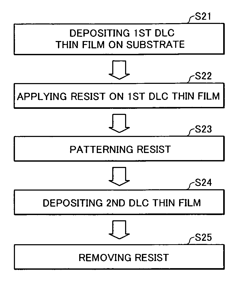
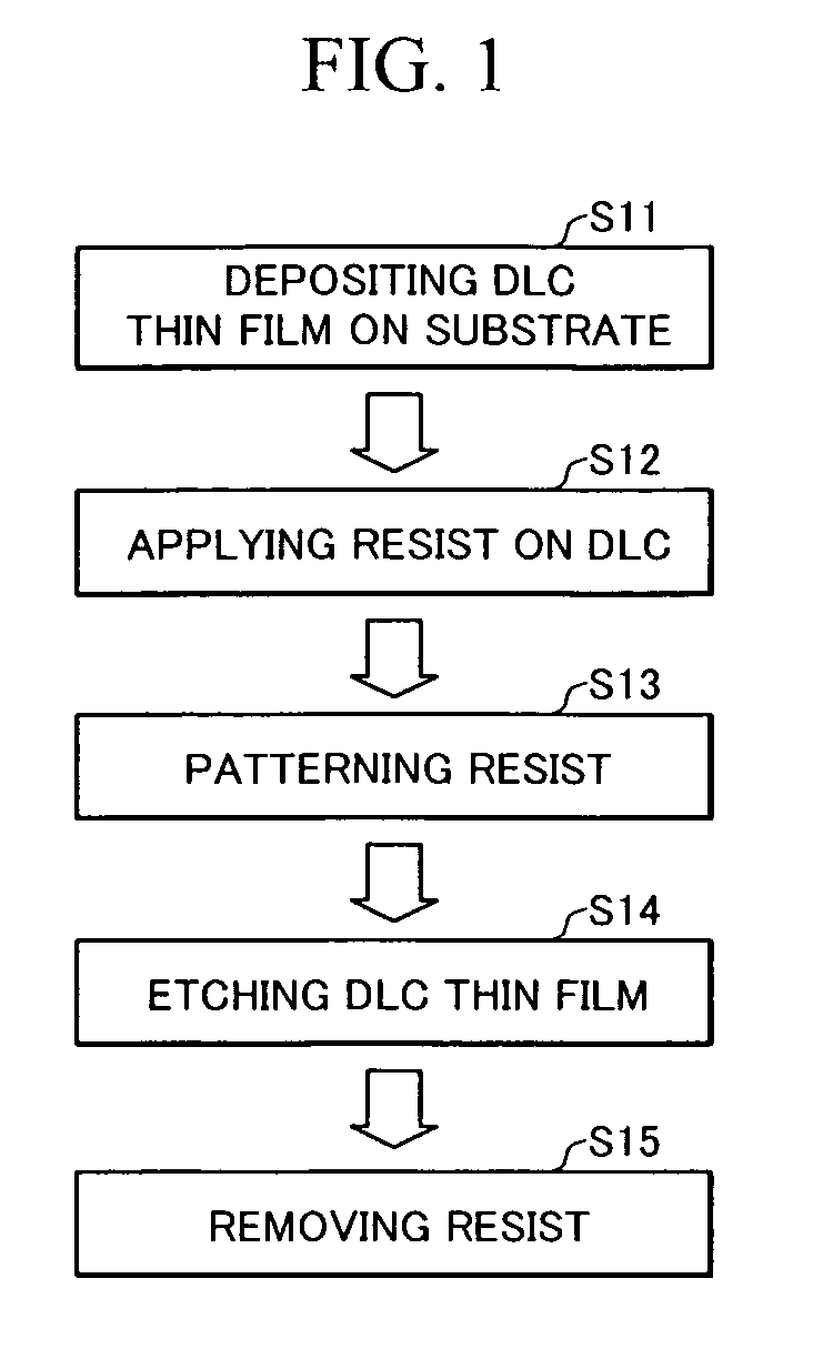
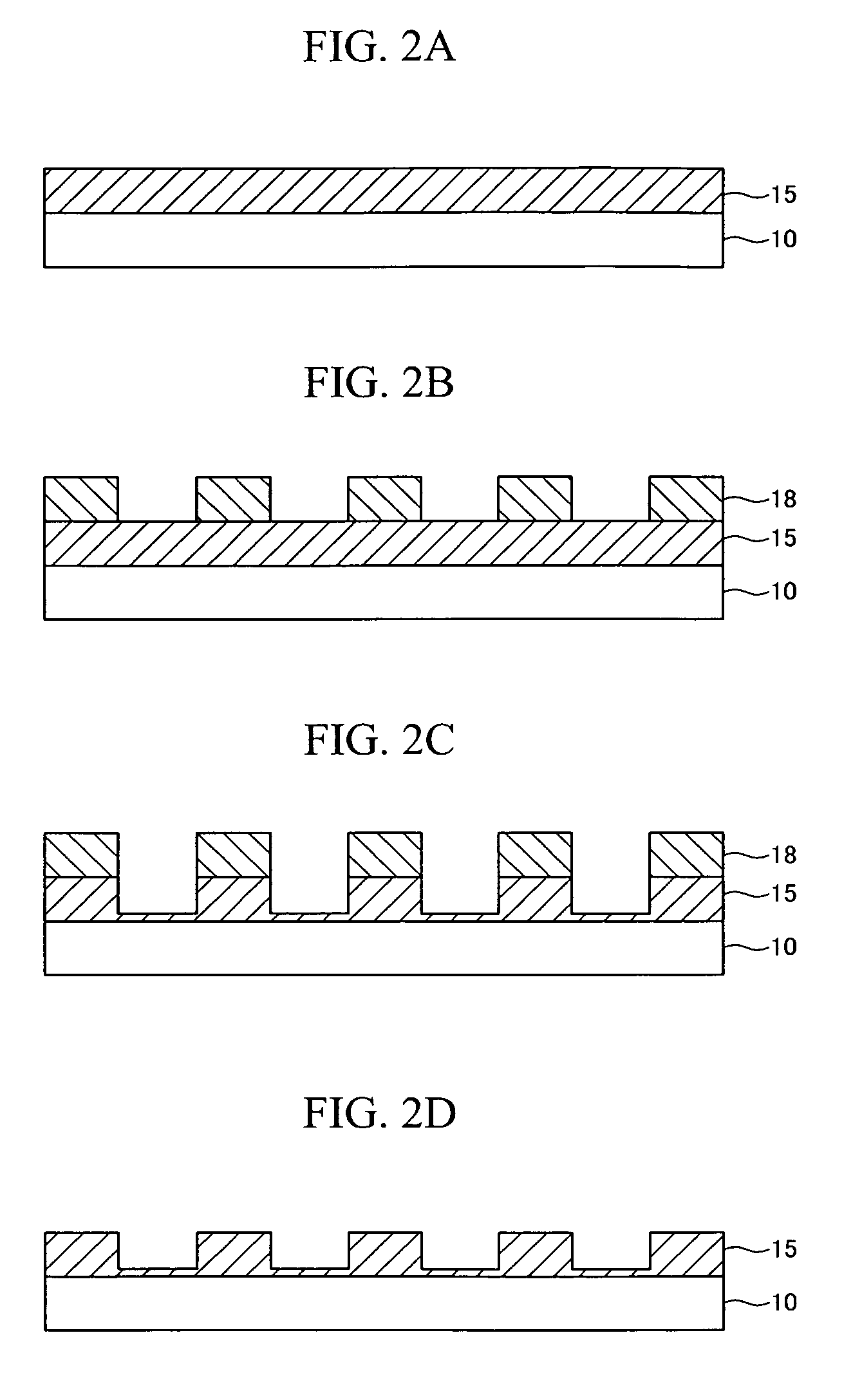
[0046]For fabricating a stamp according to a first embodiment of the present invention, as shown in FIGS. 1 and 2, a thin film 15 of diamond-like carbon (DLC) is firstly deposited on a substrate 10 (S11).

[0047]The deposition of the DLC thin film 15 may be carried out by a process selected from ion plating, plasma chemical vapor deposition (CVD) using direct current (DC) or radio frequency (RF), sputtering using DC, RF or ion-beam, and laser synthesis.

[0048]The substrate 10 may be made of a light-transmittable material that may be one of, for example, quartz, glass, diamond, a transparent polymer and a transparent semiconductor such as indium tin oxide (ITO). In an ultraviolet (UV) micro / nano imprint lithography process, in particular, the substrate 10 partly composing the stamp is preferably made of a light-transmittable material in order to transmit ultravio...


PUM

PropertyMeasurementUnit
wavelengthaaaaaaaaaa
line-widthaaaaaaaaaa

Abstract

The present invention relates to a micro / nano imprint lithography technique and in particular, to a stamp that is used in an UV-micro / nano imprint lithography process or thermal micro / nano imprint lithography process and a method for fabricating the stamp.The method for fabricating a stamp for micro / nano imprint lithography of the present invention includes i) depositing a thin film of diamond-like carbon on a substrate, ii) applying resist on the diamond-like carbon thin film, iii) patterning the resist, iv) etching the diamond-like carbon thin film by using the resist as a protective layer, and v) removing the resist.

Description

CROSS-REFERENCE TO RELATED APPLICATIONS[0001]The present application claims priority to Korean patent application No. 10-2005-0098080 filed in the Korean Intellectual Property Office on Oct. 18, 2005, and all the benefits accruing therefrom under 35 U.S.C. §119, the contents of which are herein incorporated by reference in their entirety.BACKGROUND OF THE INVENTION[0002](a) Field of the Invention[0003]The present invention relates to a micro / nano imprint lithography technique and in particular, to a stamp that is used in an UV-micro / nanoimprint lithography process or thermal micro / nano imprint lithography process and a method for fabricating the stamp.[0004](b) Description of the Related Art[0005]Micro / nano imprint lithography is a technique to fabricate micro / nano-structures effectively and economically and uses a stamp with embossed micro / nano-structure thereon in a manner that the stamp is pressed on the surface of resist applied on a substrate for imprinting the micro / nano-struc...

Claims


Application Information

Patent Timeline
Patent Type & Authority Patents(United States)
IPC IPC(8): B44C1/22
CPCB82Y10/00B82Y40/00G03F7/0002
Inventor JEONG, JUN-HOSIM, YOUNG-SUKKIM, KI-DONCHOI, DAE-GEUNLEE, EUNG-SUG
Owner KOREA INST OF MACHINERY & MATERIALS
Why Eureka
Try Eureka