

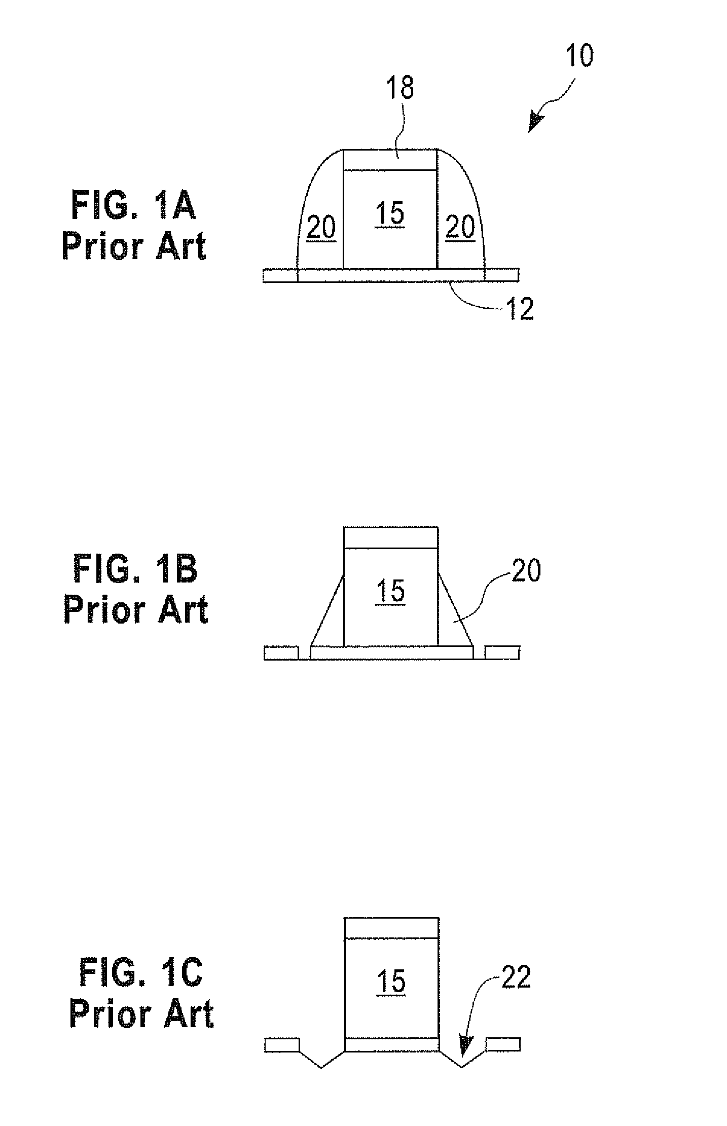
Dielectric spacer removal
a technology of dielectric spacers and dielectric plates, which is applied in the direction of semiconductor devices, electrical apparatus, transistors, etc., can solve the problems of limiting technology, lateral etch/undercut which is inherent in wet etch processes at the gate level cannot be tolerated at the pitch used in advanced technologies, and the etch rate is very low, so as to facilitate different applications of stress engineering, reduce the likelihood of electrical contact failure, and enhance mobility
- Summary
- Abstract
- Description
- Claims
- Application Information
AI Technical Summary
Benefits of technology
Problems solved by technology
Method used
Image

Examples
Embodiment Construction
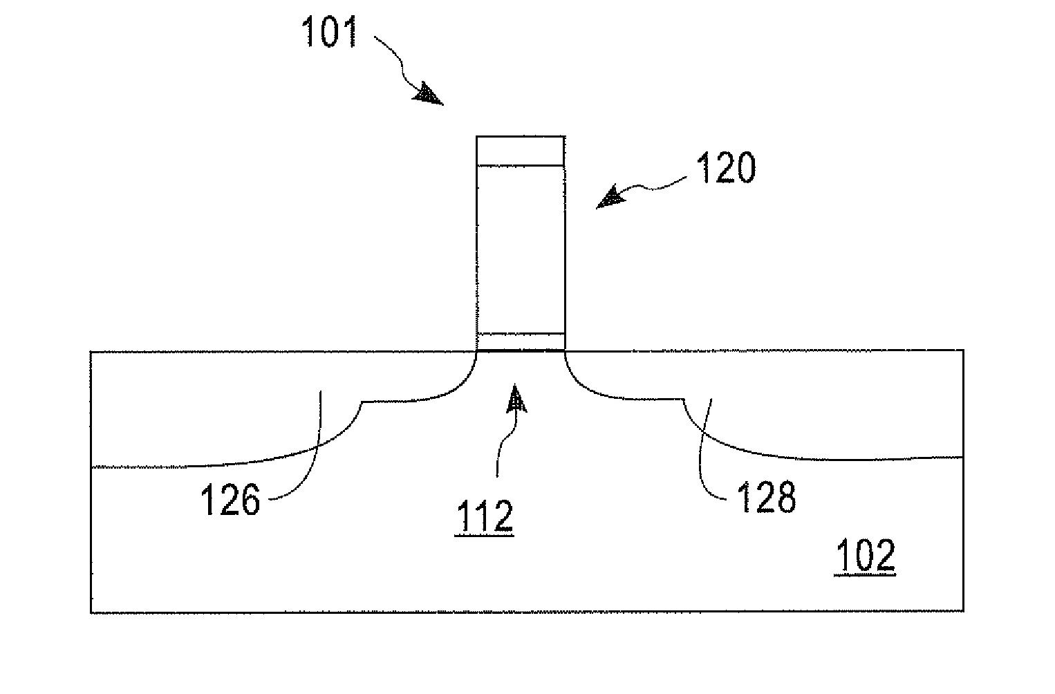
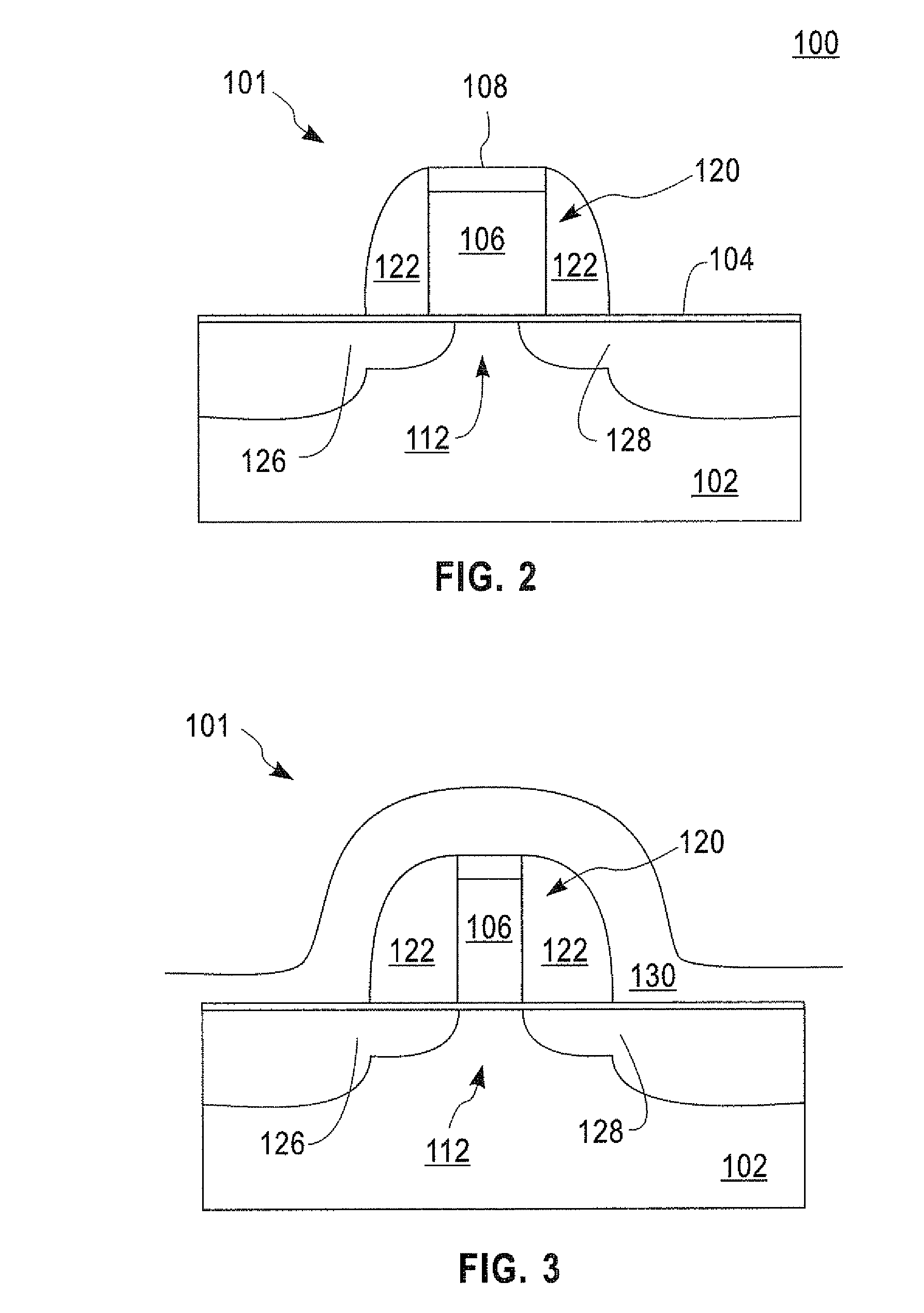
[0050]The present invention, which provides a semiconductor device comprising a semiconductor substrate having substantially no recesses in the semiconductor substrate after dielectric spacer removal, as well as a method of fabricating the same will now be described in greater detail by referring to the drawings that accompany the present application. It is noted that the drawings of the present application are provided for illustrative purposes and are thus not drawn to scale. Moreover, like and corresponding elements shown in the drawings are referred to by like reference numerals.
[0051]Reference is made to FIGS. 2-6, which are cross sectional views of a semiconductor structure during various stages of an embodiment of the present invention. Although the drawings show the presence of a single gate (i.e., a CMOS transistor structure with either pFET and / or nFET transistors), the present invention is not limited to that number of gates. Instead, the present integration process works...
PUM
 Abstract
Description
Claims
Application Information