High-performance tandem white OLED
a light-producing oled, high-performance technology, applied in the direction of discharge tube/lamp details, luminescent screen, discharge tube/lamp details, etc., can solve the problems of difficult to achieve light emission with strong intensity, weak green and red color components of tandem white oled devices, etc., to improve luminance stability and improve efficiency. , the effect of good lifetim
- Summary
- Abstract
- Description
- Claims
- Application Information
AI Technical Summary
Benefits of technology
Problems solved by technology
Method used
Image
Examples
example 2 (
INVENTIVE)
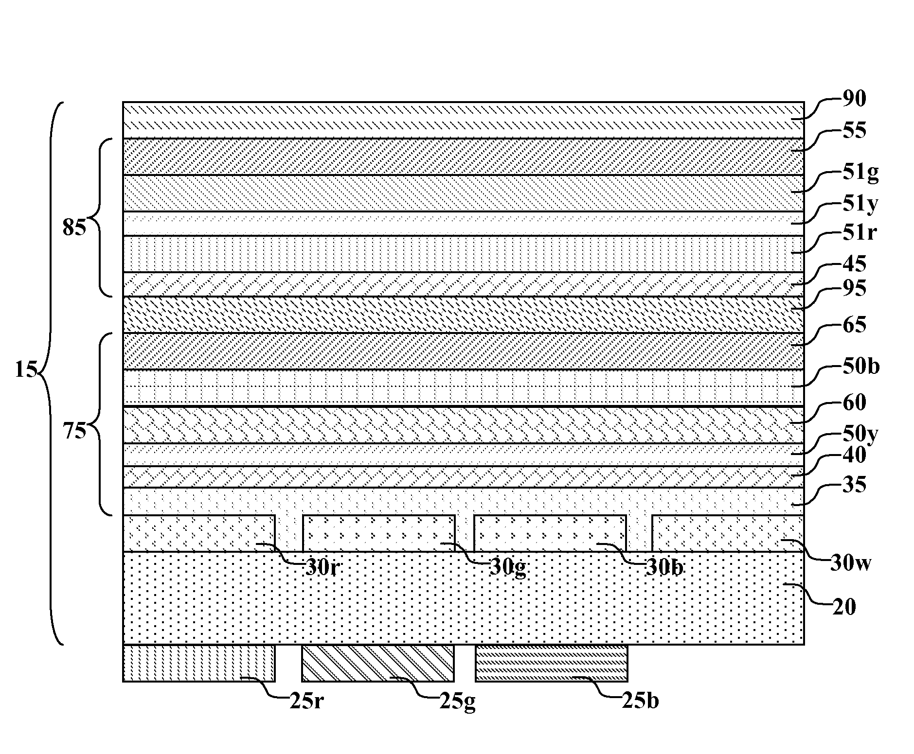
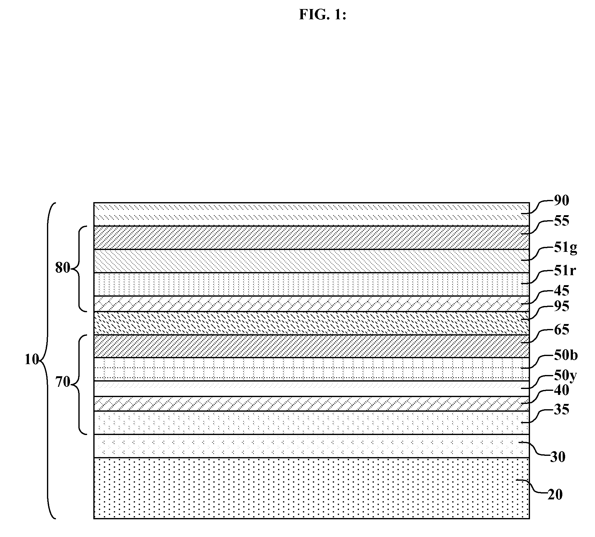
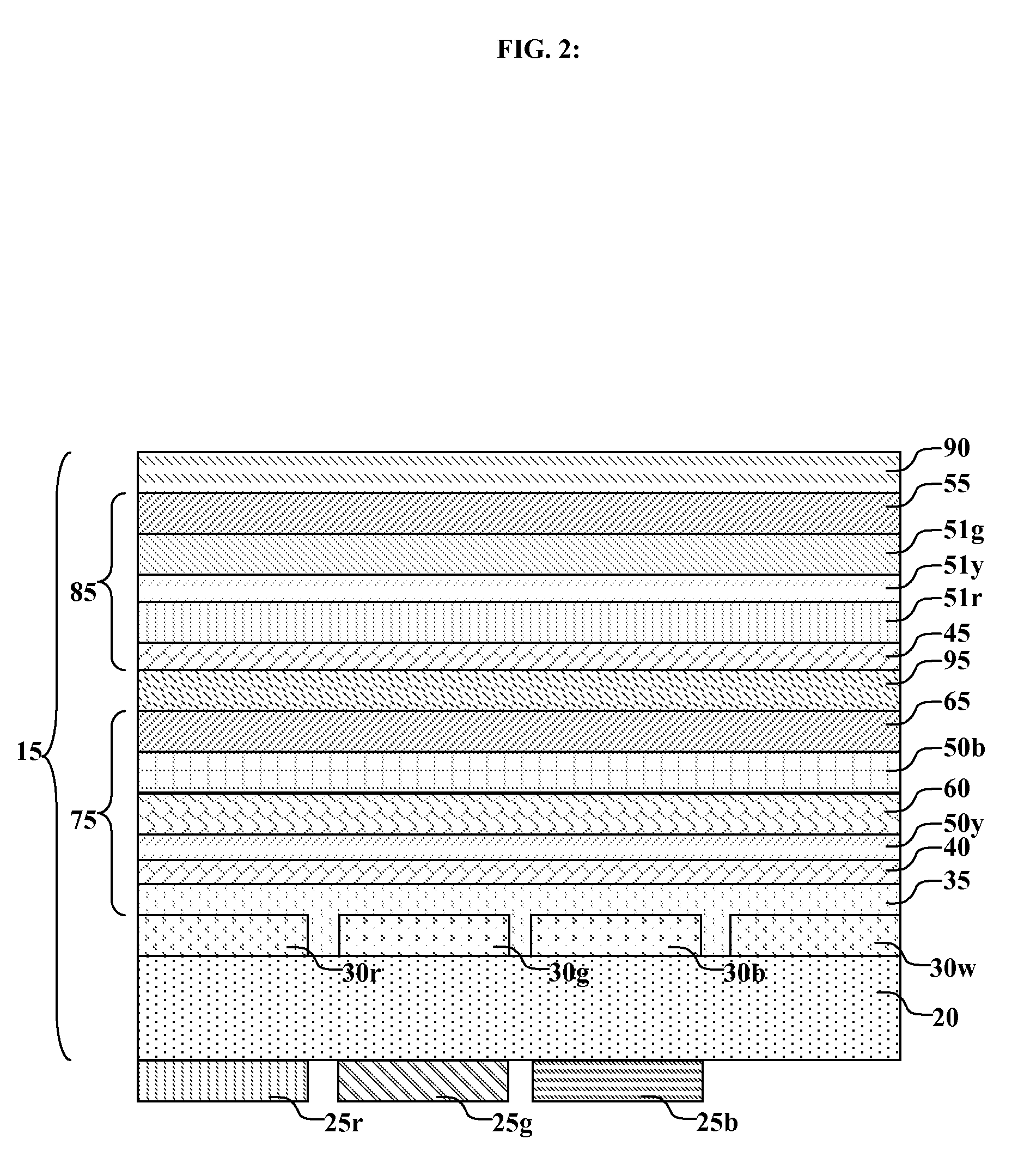
[0122]1. A clean glass substrate was deposited by sputtering with ITO to form a transparent electrode of 60 nm thickness.[0123]2. The above-prepared ITO surface was treated with a plasma oxygen etch.[0124]3. The above-prepared substrate was further treated by vacuum-depositing a 10 nm layer of CHATP as an HIL.[0125]4. The above-prepared substrate was further treated by vacuum-depositing a 130 nm layer of NPB as an HTL.[0126]5. The above-prepared substrate was further treated by vacuum-depositing a 20 nm yellow light-emitting layer including 13 nm 9-(1-naphthyl)-10-(2-naphthyl)anthracene (NNA) as host and 7 nm NPB as a co-host with 2% yellow-orange emitting dopant PTBR.[0127]6. The above-prepared substrate was further treated by vacuum-depositing a 10 nm spacer layer including 7.5 nm NNA and 2.5 nm NPB.[0128]7. The above-prepared substrate was further treated by vacuum-depositing a 30 nm blue light-emitting layer including 30 nm NNA host with 3% [N,N-di-p-tolylamino][2-[4-[...
example 3 (
INVENTIVE)
[0137]An OLED device was constructed as described above for Example 2 except that Step 7 was as follows:[0138]7. The above-prepared substrate was further treated by vacuum-depositing a 30 nm blue light-emitting layer including 30 nm NNA host with 3% [N,N-di-p-tolylamino][2-[4-[N,N-di-p-tolylamino]phenyl]vinyl]biphenyl and 1% BEP as blue-emitting dopants.
example 4 (
INVENTIVE)
[0139]An OLED device was constructed as described above for Example 2 except that Step 13 was as follows:[0140]13. The above-prepared substrate was further treated by vacuum-depositing a 40 nm green light-emitting layer including 36.6 nm PBNA, 3 nm 2,6-bis(diphenylamino)-9,10-diphenylanthracene as green emitting dopant, and 0.4 nm BEP as blue emitting dopant.
EXAMPLE 5 (INVENTIVE)
[0141]An OLED device was constructed as described above for Example 2 except that Step 12 was as follows:[0142]12. The above-prepared substrate was further treated by vacuum-depositing a 4 nm yellow light-emitting layer including 2 nm NNA and 2 nm NPB with 2% yellow-orange emitting dopant PTBR.
PUM
| Property | Measurement | Unit |
|---|---|---|
| wavelengths | aaaaa | aaaaa |
| wavelengths | aaaaa | aaaaa |
| wavelengths | aaaaa | aaaaa |
Abstract
Description
Claims
Application Information


