Broadband imaging device and manufacturing thereof

Inactive Publication Date: 2011-07-05
BANPIL PHOTONICS
View PDF3 Cites 64 Cited by
  • Summary
  • Abstract
  • Description
  • Claims
  • Application Information

AI Technical Summary

Benefits of technology

[0043]The invention offers to detect broad detection ranges varying from UV to mid infrared as high as long infrared wavelengths with high quantum efficiency, high frequency response, and increased signal-to-noise ratio. With proper design and fabrication process, M×N photodiode arrays can be fabricated with capability to independently addressable each photodiode. The photodiode array will have the CCD like feature with broad spectral detection capabi

Problems solved by technology

Additionally, HgCdTe is plagued by material growth issues and narrow bandgaps also of InAs and InSb, result in detectors with large dark currents at room temperature.
None of current solution can provide broad spectral detection capability ranges from UV to l

Method used


Image

  • Broadband imaging device and manufacturing thereof
  • Broadband imaging device and manufacturing thereof
  • Broadband imaging device and manufacturing thereof

Examples


Embodiment Construction

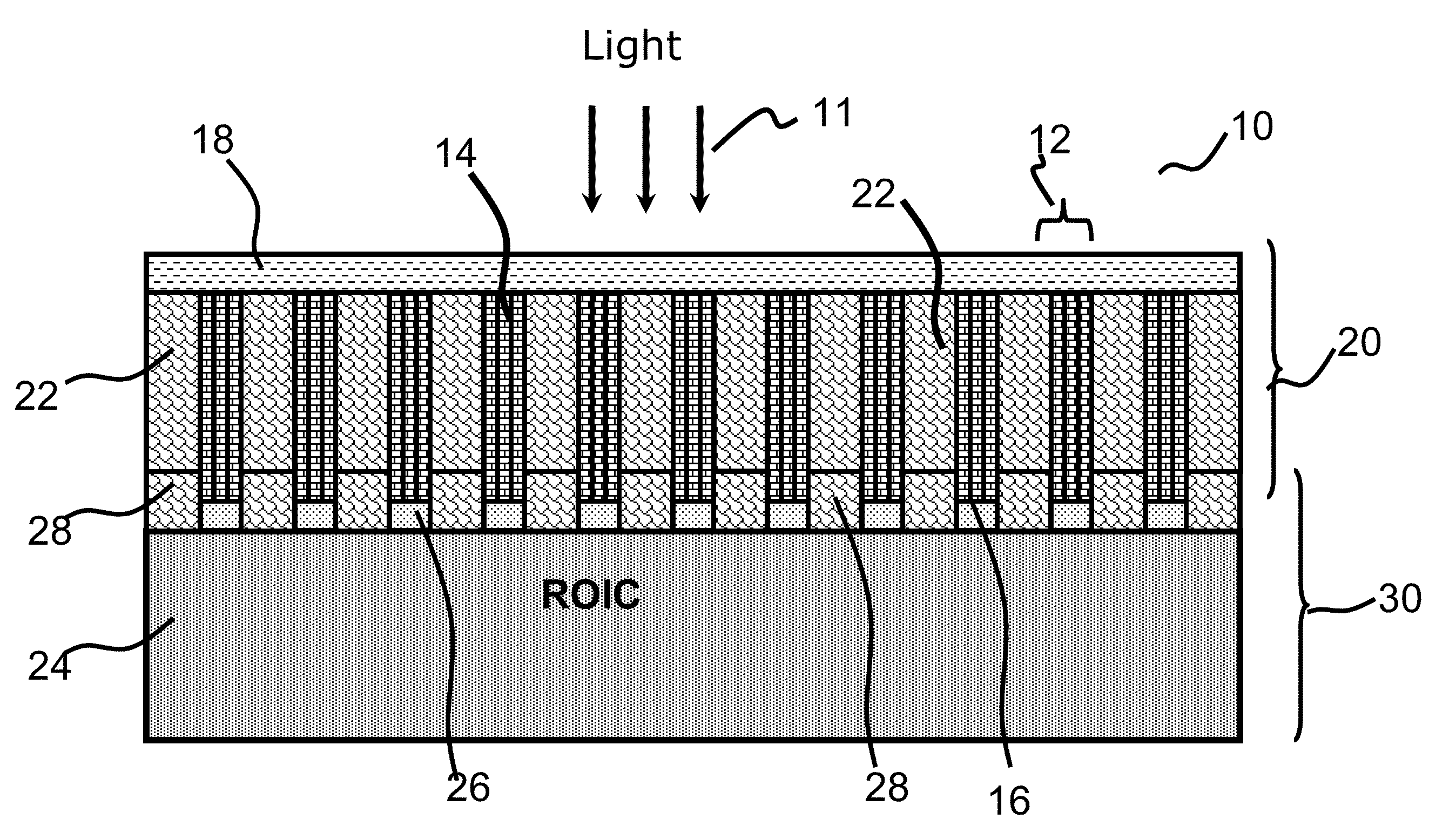
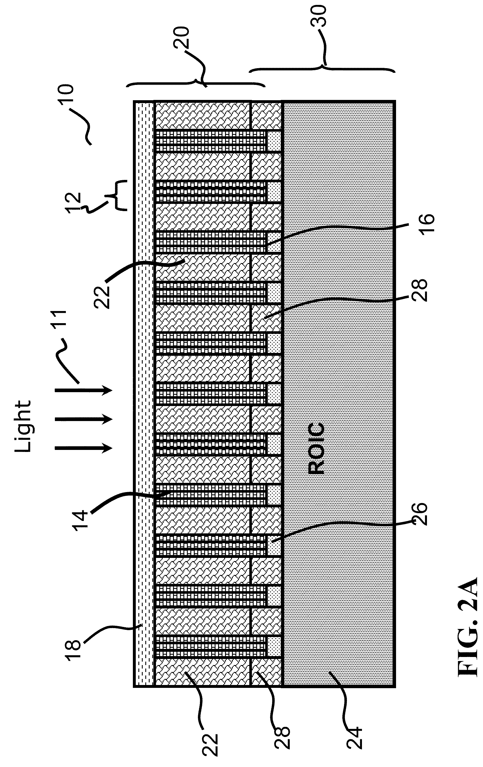
[0058]The best modes for carrying out the present invention will be described in terms with reference to the accompanying drawings. In the following description, the same reference numerals denote components having substantially the same functions and arrangements, and duplicate explanation will be made only where necessary.

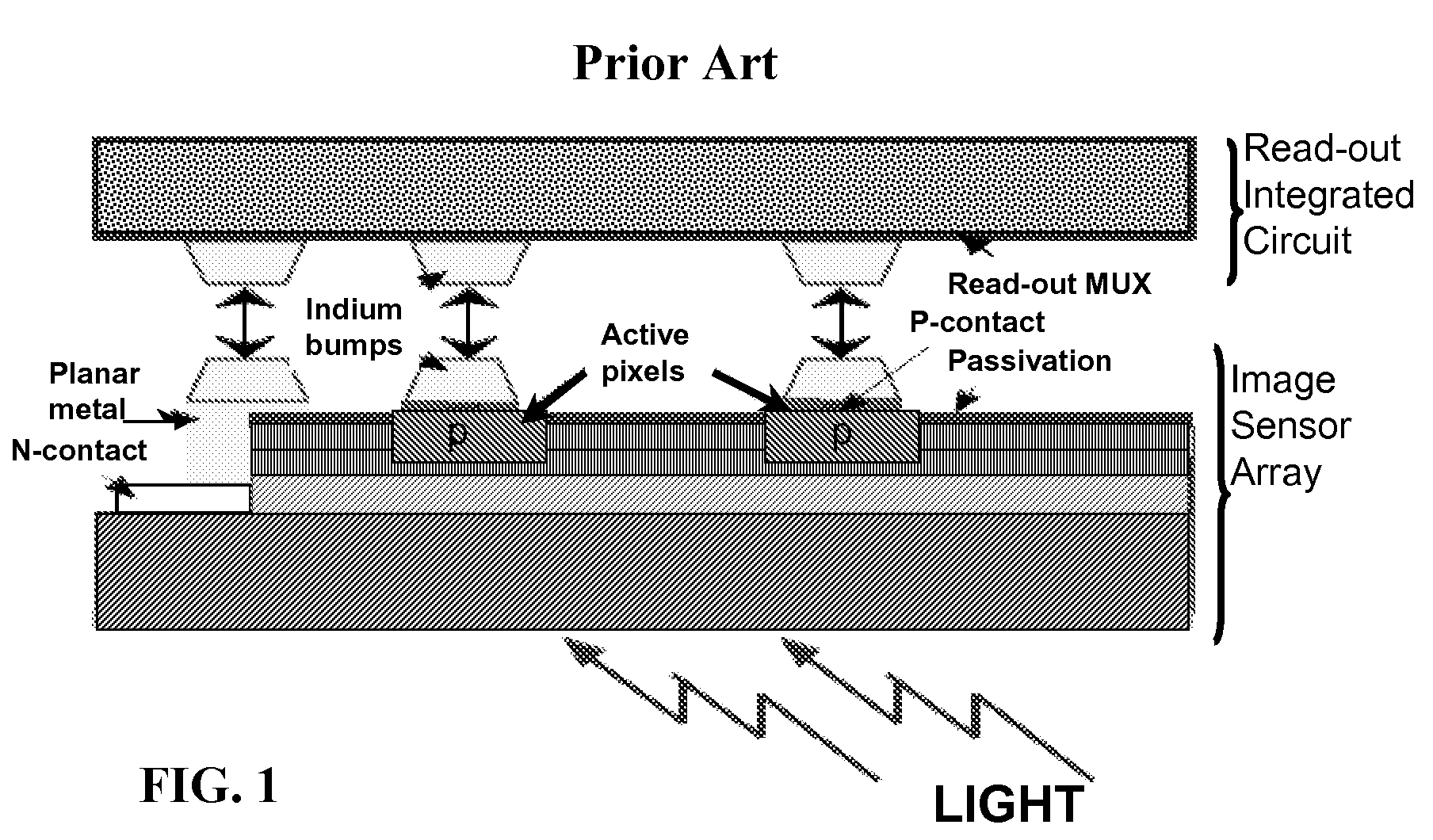
[0059]Here the structure and design we mention, are for both top (also mentioned as ‘front’)-illuminated and bottom (also mentioned as ‘back’)-illuminated type image sensor and their array having broad spectral detection ranges. The main objective of this invention is to make the broad spectral array from any material systems such as Si, Ge, SiGe, GaN, GaAs, InP, InGaAs, InAs, HgCdTe, CdTe, ZnCdTe, PbS etc. This covers all sensor and its array with broad spectral detection ranges which covers from <300 nm (or as low as UV to long-Infrared (10 μm and more longer) wavelengths range. This invention also cover the sensors and their array's transferring technology to ...


PUM


Abstract

This invention relates to imaging device and its related transferring technologies to independent substrate able to attain significant broadband capability covering the wavelengths from ultra-violet (UV) to long-Infrared. More particularly, this invention is related to the broadband image sensor (along with its manufacturing technologies), which can detect the light wavelengths ranges from as low as UV to the wavelengths as high as 20 μm covering the most of the wavelengths using of the single monolithic image sensor on the single wafer. This invention is also related to the integrated circuit and the bonding technologies of the image sensor to standard integrated circuit for multicolor imaging, sensing, and advanced communication. Our innovative approach utilizes surface structure having more than micro-nano-scaled 3-dimensional (3-D) blocks which can provide broad spectral response. Utilizing multiple micro-nano scaled blocks help to increase the absorption spectra more than the material used as the absorption layer. In addition, utilizing the multiple nano-scaled 3-D blocks help to increase the absorption over the wavelength due to the multiple reflections and diffractions inside the 3-D structures. The absorption layers will be designed to achieve the required quantum efficiency and also required speed.

Description

CROSS REFERENCE TO RELATED APPLICATIONS[0001]This application claims the benefit of U.S. Provisional Application No. 61 / 099,910 filed on Sep. 25, 2008.FIELD OF THE INVENTION[0002]This invention relates to imaging device and its related transferring technologies to independent substrate able to attain significant broadband capability covering the wavelengths from ultra-violet (UV) to long-Infrared. More particularly, this invention is related to the broadband image sensor (along with its manufacturing technologies), which can detect the light wavelengths ranges from as low as UV to the wavelengths as high as 20 μm covering the most of the wavelengths using of the single monolithic image sensor on the single wafer. This invention is also related to the integrated circuit and the bonding technologies of the image sensor to standard integrated circuit for multicolor imaging, sensing, and advanced communication.BACKGROUND OF THE INVENTION[0003]Solid-state imaging devices with higher reso...

Claims


Application Information

Patent Timeline
IPC IPC(8): H01L21/00
CPCB82Y20/00H01L27/14634H01L31/0352H01L31/035236H01L31/035281H01L31/18Y02E10/50
Inventor DUTTA, ACHYUT KUMAROLAH, ROBERT ALLEN
Owner BANPIL PHOTONICS
Why Eureka
Try Eureka