Semiconductor device manufacturing method
a technology of semiconductor devices and manufacturing methods, applied in the direction of domestic cooling devices, lighting and heating devices, applications, etc., can solve the problems of increasing the temperature distribution over the substrate, difficult to maintain the uniformity of etching rate, and increasing apparatus costs, so as to achieve stable processing and efficient and uniform cooling or heating portions
- Summary
- Abstract
- Description
- Claims
- Application Information
AI Technical Summary
Benefits of technology
Problems solved by technology
Method used
Image
Examples
first embodiment
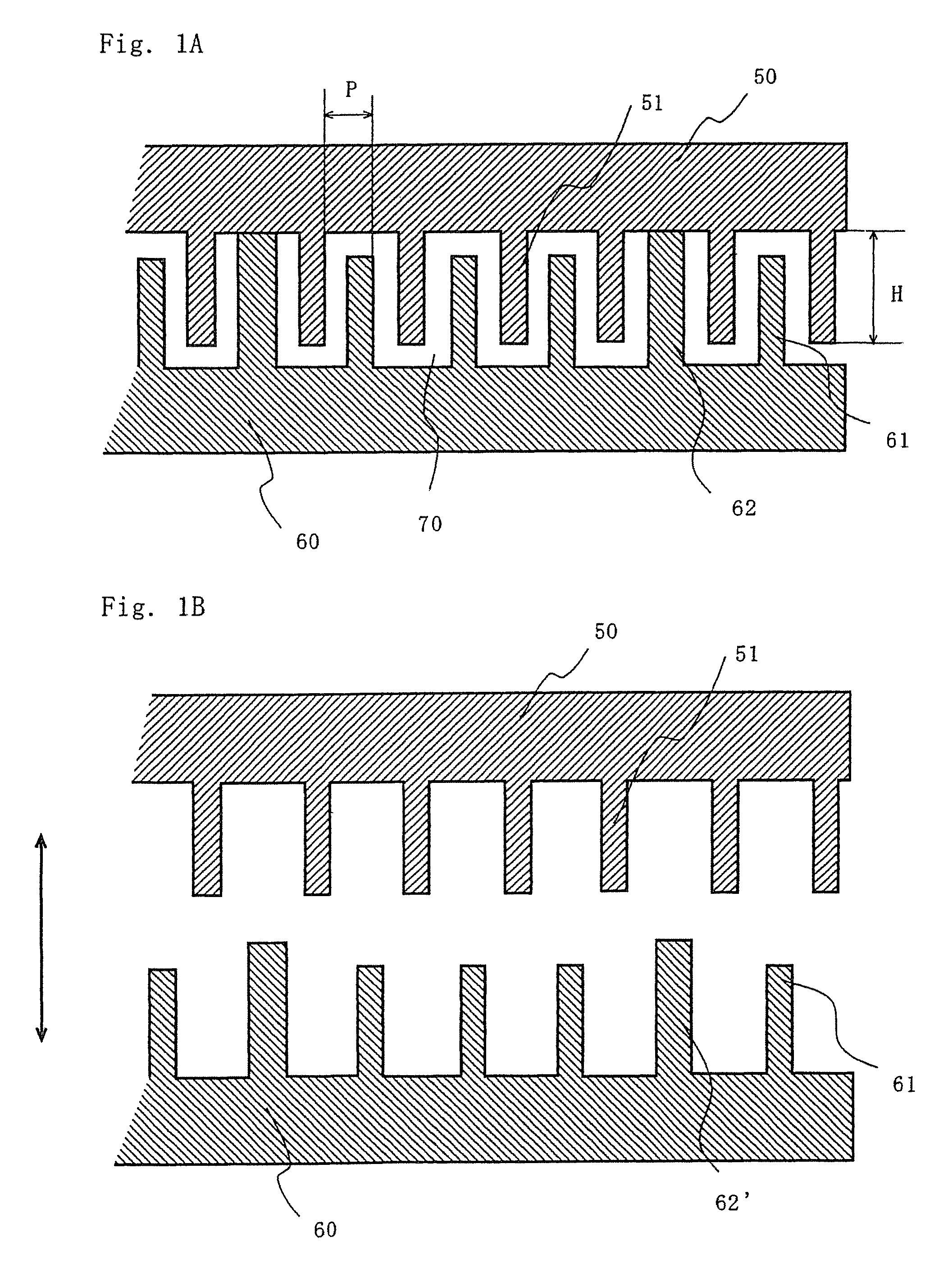
[0029]this invention is shown in FIG. 1. FIG. 1 is a schematic sectional view showing a part of heat exchanger used for a substrate processing apparatus of this invention.
[0030]In a heat exchanger shown in FIG. 1A, the space between two plates 50, 60 is divided with partition walls (fluid channel walls) 62 to form a fluid channel 70. A fluid introduction port and an exhaust port (not illustrated) are disposed at respective ends of the fluid channel. Moreover, a lot of fins 51, 61 are arranged on upper plate 50 and lower plate 60 inside the channel.
[0031]The height of the fin is set so that the ends of upper plate fins 51 and the lower plate fins 61 overlap each other. The inside of channel is not separated completely by the upper plate fins 51 or the lower plate fins 61 so that the fluid moves between sub-channels formed by the fins. The cooling capacity can be made uniform over the entire heat exchanger even when each sub-channel has a different conductance.
[0032]Here, there is no ...
second embodiment
[0056]this invention is shown in FIGS. 2 and 3.
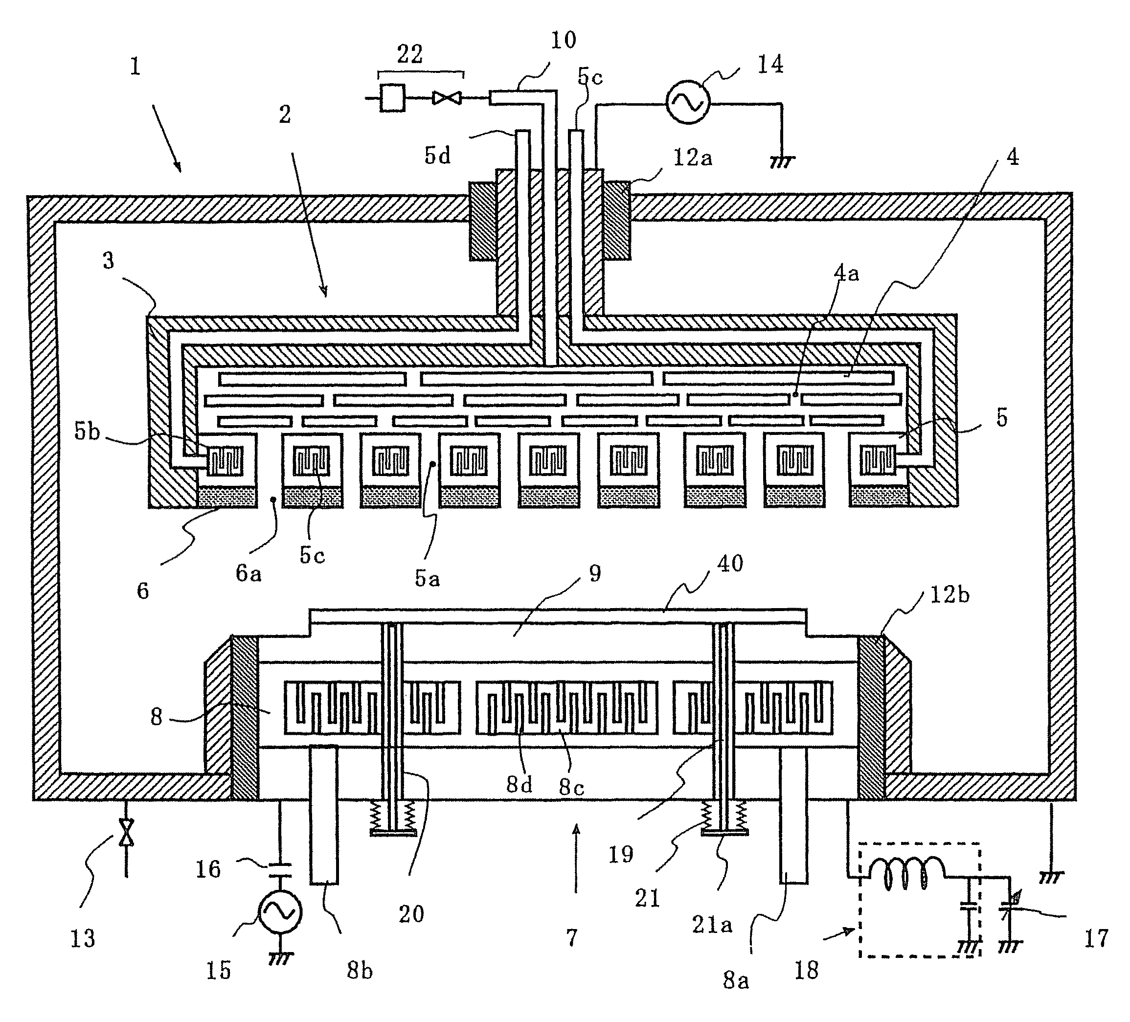
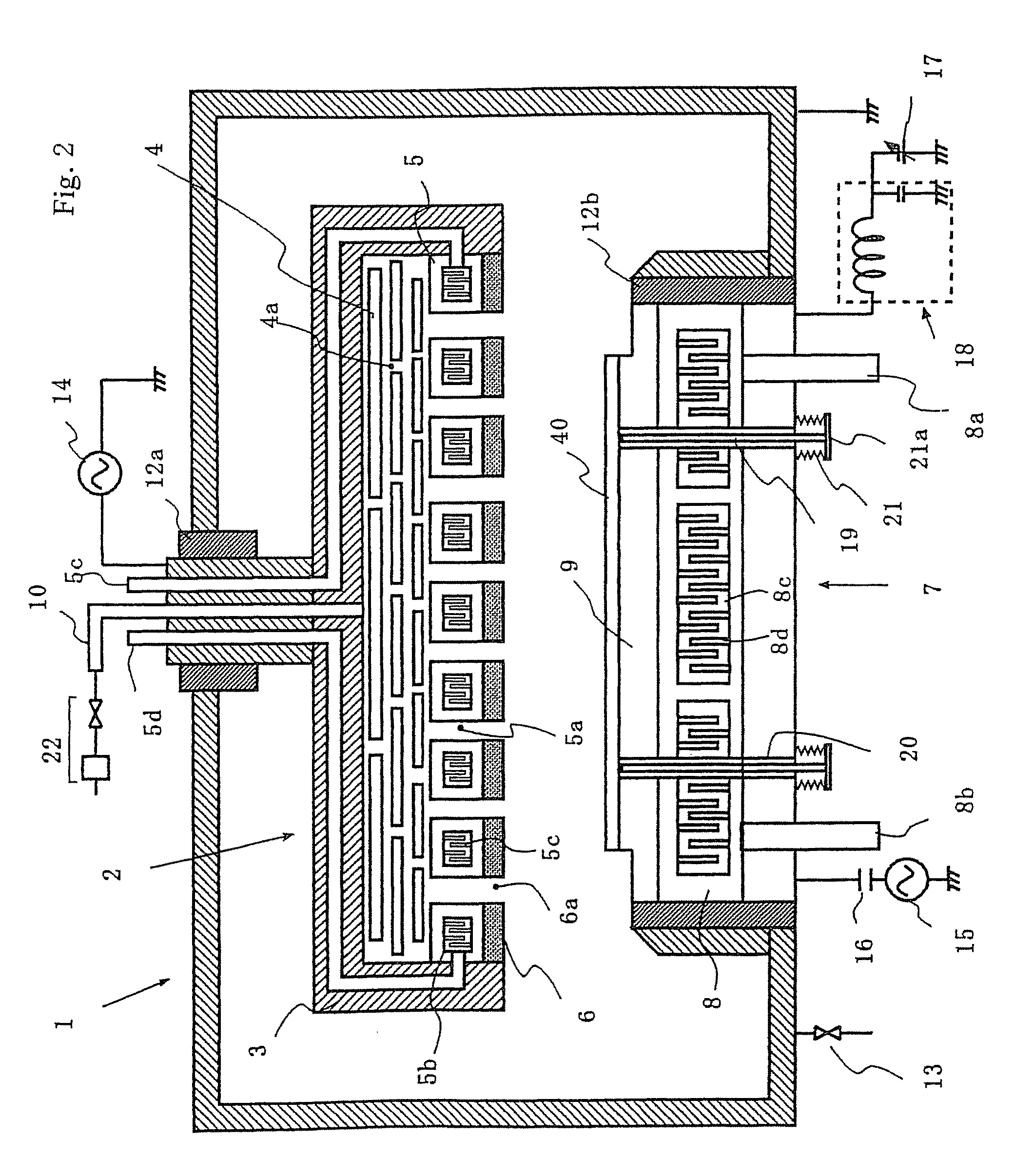
[0057]FIG. 2 is a cross sectional view showing an example of etching apparatus of this invention. As shown in FIG. 2, an opposite electrode (gas emitting means) 2 and a substrate holding electrode (substrate holder) 7 for holding a substrate 40 are arranged facing each other, and are fixed through insulators 12a and 12b in a process chamber 1 of etching apparatus, respectively. The inside of the process chamber is connected with an exhaust means (not illustrated) through a valve 13. The opposite electrode 2 is connected with a first high frequency power source 14 for generating plasma as well as with a gas introduction means comprising a gas introduction pipe 10 and a gas supply system 2 which is composed of a gas cylinder, a mass flow controller, a stop valve and the like.
[0058]The opposite electrode 2 comprises; a gas distribution mechanism in which one or a plurality of gas distribution plates 4 having a number of small holes 4a are ...
PUM
| Property | Measurement | Unit |
|---|---|---|
| angle | aaaaa | aaaaa |
| height H | aaaaa | aaaaa |
| temperature | aaaaa | aaaaa |
Abstract
Description
Claims
Application Information


