Deposition sub-chamber with variable flow

a sub-chamber and variable flow technology, applied in chemical vapor deposition coatings, coatings, metallic material coating processes, etc., can solve the problems of unfavorable uniformity, unwanted film deposition and other problems, and achieve the effect of improving the chamber performan

Active Publication Date: 2011-08-09
NOVELLUS SYSTEMS
View PDF110 Cites 262 Cited by
  • Summary
  • Abstract
  • Description
  • Claims
  • Application Information

AI Technical Summary

Benefits of technology

[0015]The present invention provides apparatus and methods for uniformly depositing film on a substrate including a plurality of conduits that allows by-product and reactant gases to flow past the edge

Problems solved by technology

Conventional ALD, however, depends on self-limiting, typically-monolayer-producing reactions for both reactant gases.
Since the precursors are not put into the same deposition space (chamber or chamber region), they do not readily react to deposit and accumulate film on the walls of the chamber.
Even with the separation of the deposition spaces within the main reactor chamber and dual seal design, unwanted film deposition and uniformity issues can still occur.
As described above, the film deposition reaction is catalytically-assisted and self-limiting.
Very high chamber pressure can be problematic when the chamber seal disengages and the pressure quickly reduces to vacuum.
A large flow of by-product gas and remaining reactant gas may float and then drop the wafer, causing orientation and positioning problems.
Also the wafer movement may damage the wafer and result in unwanted particles in the chamber or on the wafer.
This may result in chemical

Method used


Image

  • Deposition sub-chamber with variable flow
  • Deposition sub-chamber with variable flow
  • Deposition sub-chamber with variable flow

Examples


Embodiment Construction

[0035]In the following detailed description of the present invention, numerous specific embodiments are set forth in order to provide a thorough understanding of the invention. However, as will be apparent to those skilled in the art, the present invention may be practiced without these specific details or by using alternate elements or processes. In other instances, well-known processes, procedures and components have not been described in detail so as not to unnecessarily obscure aspects of the present invention.

INTRODUCTION

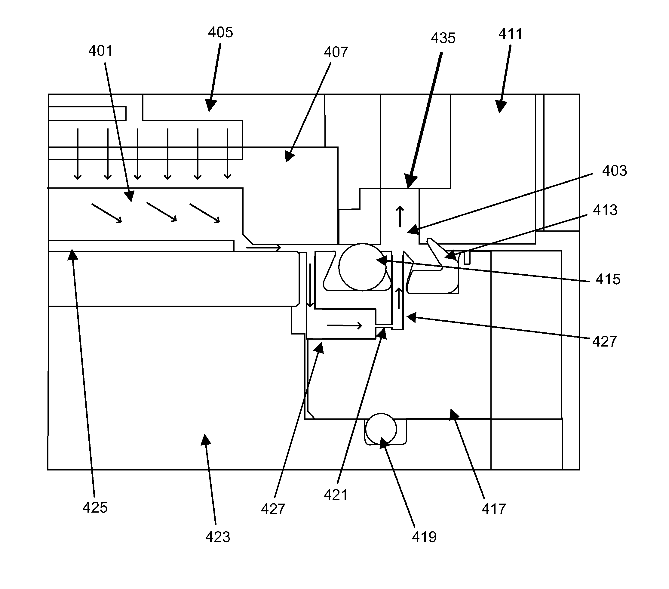
[0036]As indicated, the present invention provides apparatus and associated methods for conducting a chemical deposition. The apparatus and methods are particularly applicable to use in conjunction with a semiconductor fabrication based dielectric deposition process that requires separation of self-limiting deposition steps in a multi-step deposition process (e.g., atomic layer deposition (ALD) or pulsed deposition layer (PDL) processing for catalyst and silico...


PUM

PropertyMeasurementUnit
Fractionaaaaaaaaaa
Diameteraaaaaaaaaa
Volumeaaaaaaaaaa

Abstract

An apparatus and method for depositing film on a substrate includes a plurality of conduits that allow by-product and reactant gases to flow past the edge of a substrate. The apparatus and process of the present invention has several advantages for enhanced chamber performance, particularly for micro-volume chambers using pulsed deposition layer processes.

Description

FIELD OF THE INVENTION[0001]This invention pertains to apparatuses and processes for conducting chemical depositions, and may find particular use in depositing a conformal film of dielectric material with a high degree of surface smoothness and uniformity particularly suited, but not limited, to high aspect ratio features in semiconductor device fabrication.BACKGROUND OF THE INVENTION[0002]Conformal, uniform dielectric films have many applications in semiconductor manufacturing. In the fabrication of sub-micron integrated circuits (ICs) several layers of dielectric film are deposited. Four such layers are shallow trench isolation (STI), pre-metal dielectric (PMD), inter-metal dielectric (IMD) and interlayer dielectric (ILD). Other applications of conformal dielectric films may be as sacrificial or permanent spacer layers, sacrificial or permanent storage node separation layers, or as dielectric liners for through-wafer vias. All of these layers require silicon dioxide or other diele...

Claims


Application Information

Patent Timeline
IPC IPC(8): C23C16/458H01L21/306C23F1/00C23C16/06C23C16/22
CPCC23C16/45517C23C16/45544
Inventor KROTOV, PETERSMITH, COLIN F.
Owner NOVELLUS SYSTEMS
Why Eureka
Try Eureka