
Method for fabricating gallium nitride based semiconductor electronic device

a gallium nitride-based semiconductor and electronic device technology, applied in semiconductor devices, diodes, electrical devices, etc., can solve the problems of warpage of support and gallium nitride-based semiconductor layers, adversely affecting adhesiveness, etc., to reduce warpage, reduce stress relaxation effect, and reduce the yield of semiconductor chips

Inactive Publication Date: 2011-08-16
SUMITOMO ELECTRIC IND LTD
View PDF6 Cites 17 Cited by
  • Summary
  • Abstract
  • Description
  • Claims
  • Application Information

AI Technical Summary

Benefits of technology

[0008]In view of the circumstances above, an object of the present invention is to provide a method of fabricating a gallium nitride-based semiconductor electronic device, the method preventing a reduction in adhesiveness between a gallium nitride-based semiconductor layer and a conductive substrate.
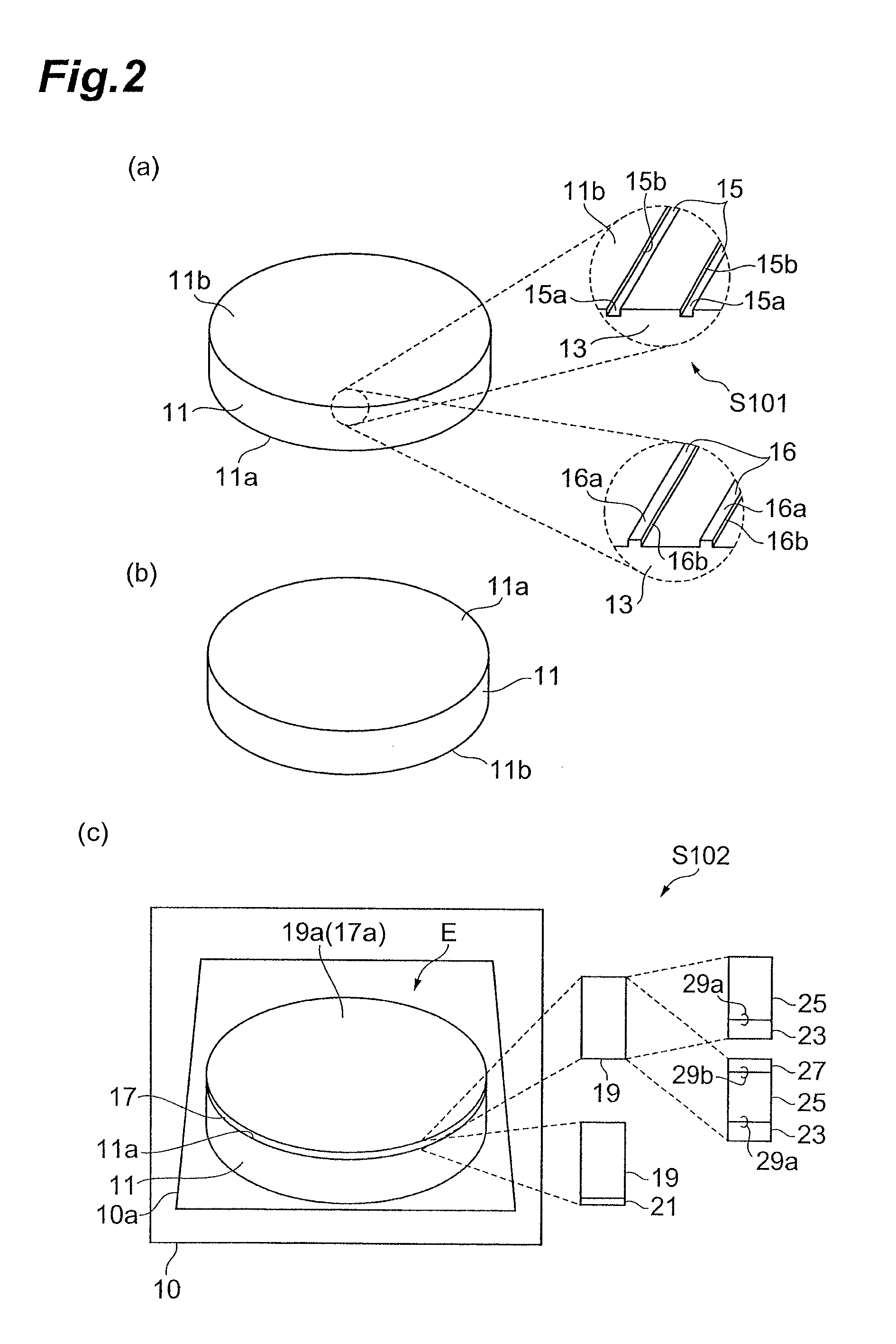
[0018]The support may include one of sapphire, silicon carbide, and aluminum nitride in the method. The support of one of such materials facilitates favorable crystal growth and excellent warpage reduction.

Problems solved by technology

During deposition of a gallium nitride-based semiconductor layer on the support comprising a different material, however, the support and the gallium nitride-based semiconductor layer warp due to stress, unlike deposition on the GaN substrate.
The inventors found that the warpage adversely affects the adhesiveness between the gallium nitride-based semiconductor layer and a conductive substrate in a process of bonding the conductive substrate to the gallium nitride-based semiconductor layer on the support comprising the different material.

Method used


Image

  • Method for fabricating gallium nitride based semiconductor electronic device
  • Method for fabricating gallium nitride based semiconductor electronic device
  • Method for fabricating gallium nitride based semiconductor electronic device

Examples


example 1

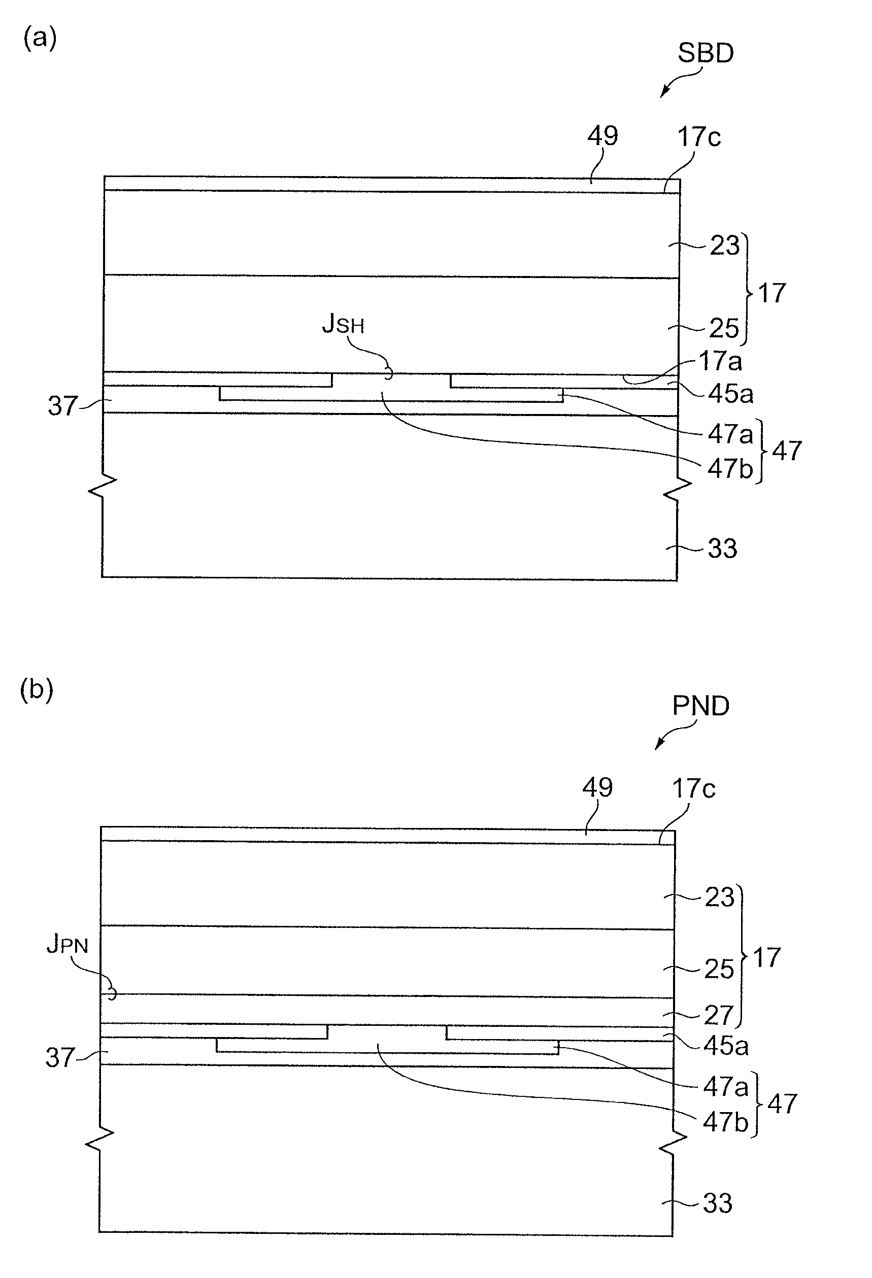
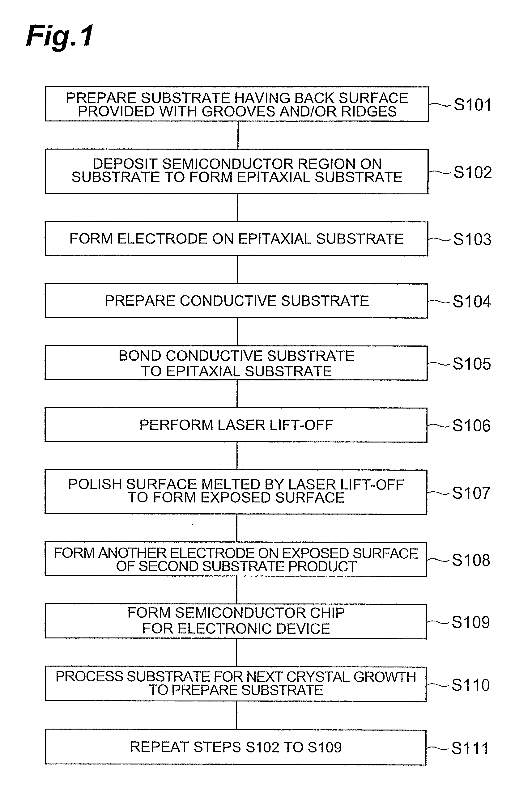
[0069]An aluminum nitride substrate is prepared. An array of grooves is provided in the back surface of the aluminum nitride substrate, the grooves having a width of 10 μm, a depth of 10 μm, and a pitch of 5,000 μm. An n+-type gallium nitride layer having a carrier concentration of 1×1018 cm−3 is formed on the principal surface of the aluminum nitride substrate by fluxing. The gallium nitride layer has a thickness of 20 μm. Subsequently, an n−-type gallium nitride layer having a carrier concentration of 7×1015 cm−3 is deposited by MOCVD. The gallium nitride layer has a thickness of 5 μm. After the epitaxial substrate is removed from a growth furnace, a field plate structure including silicon nitride and a Schottky electrode are formed on the surface of an epitaxial film of the epitaxial substrate. The field plate structure includes a silicon nitride film. The Schottky electrode includes Au / Ni, for example. The Schottky electrode forms a Schottky junction with the surface of the epit...

example 2

[0070]A sapphire substrate is prepared. An array of grooves is provided in the back surface of the sapphire substrate, the grooves having a width of 20 μm, a depth of 50 μm, and a pitch of 1,000 μm. An InGaN layer having a high proportion of indium (0.07) is formed as a buffer layer on the sapphire substrate by MOCVD. Subsequently, an n+-type gallium nitride layer having a carrier concentration of 1×1018 cm−3 and a thickness of 10 μm, an n−-type gallium nitride layer having a carrier concentration of 7×1015 cm−3 and a thickness of 5 μm, and a p-type gallium nitride layer having a carrier concentration of 1×1017 cm−3 and a thickness of 2 μm are formed to provide an epitaxial substrate including a layer structure. The epitaxial substrate and a Mo support base are joined, and then the back surface of the sapphire substrate is irradiated with YAG laser light. The YAG laser light, which is absorbed at a high absorption rate in the InGaN buffer layer having a high proportion of indium, re...

example 3

[0071]In Example 1, a sapphire substrate is prepared having a back surface in which grooves are provided in a lattice shape at a pitch corresponding to a device size. In Example 3, the pitch of the grooves is 1.5 mm. A semiconductor region of a gallium nitride-based semiconductor is deposited on the principal surface of the sapphire substrate as in Example 1. Since the substrate is grooved, the sapphire substrate and an epitaxial film are strained and warped after crystal growth, due to a difference in coefficient of thermal expansion between the sapphire substrate and the epitaxial film. The strain is relieved by the array of grooves in the back surface of the sapphire substrate, and thus adhesiveness in bonding of the substrate to a conductive support base is improved. Accordingly, diodes are produced at an excellent yield.


PUM

PropertyMeasurementUnit
carrier concentrationaaaaaaaaaa
depthaaaaaaaaaa
depthaaaaaaaaaa

Abstract

A method of fabricating a gallium nitride-based semiconductor electronic device is provided, the method preventing a reduction in adhesiveness between a gallium nitride-based semiconductor layer and a conductive substrate. A substrate 11 is prepared. The substrate 11 has a first surface 11a and a second surface 11b, the first surface 11a allowing a gallium nitride-based semiconductor to be deposited thereon. The substrate 11 includes a support 13 of a material different from the gallium nitride-based semiconductor. The support is exposed on the second surface 11b of the substrate 11. An array of grooves 15 is provided in the second surface 11b. A semiconductor region including at least one gallium nitride-based semiconductor layer is deposited on the first surface 11a of the substrate 11, and thereby an epitaxial substrate E is fabricated. A conductive substrate 33 is bonded to the epitaxial substrate E such that the semiconductor region 17 is provided between the first surface 11a of the substrate 11 and the conductive substrate E. Subsequently, the second surface 11b is irradiated with laser light for laser lift-off.

Description

BACKGROUND OF THE INVENTION[0001]1. Field of the Invention[0002]The present invention relates to a method for fabricating a gallium nitride-based semiconductor electronic device.[0003]2. Related Background Art[0004]Patent Literature 1 (Japanese Unexamined Patent Application Publication No. 2007-158133) discloses a laser lift-off process. A light-emitting region, an n-type layer, and a p-type layer are formed on a sapphire substrate. An n-type silicon substrate is then prepared, and conductive multilayer films are vapor-deposited on two surfaces of the substrate. Subsequently, an electrode on the p-type layer and the conductive multilayer film on the n-type silicon substrate are hot-pressed at a temperature of 300° C. to coalesce the two substrates. The back surface of the sapphire substrate is then irradiated with laser light so that GaN on the surface of the n-type layer is decomposed. The sapphire substrate is then removed by a lift-off process.[0005]Patent Literature 2 (Japanese ...

Claims


Application Information

Patent Timeline
Patent Type & Authority Patents(United States)
IPC IPC(8): H01L21/30
CPCH01L29/66204H01L29/66219H01L29/861H01L29/872H01L29/2003
Inventor SHIOMI, HIROMUFUJIWARA, SHINSUKESAITOH, YUKIYAMA, MAKOTO
Owner SUMITOMO ELECTRIC IND LTD
Learn More