Semiconductor device

a technology of semiconductor devices and semiconductors, applied in semiconductor devices, semiconductor/solid-state device details, electrical apparatus, etc., can solve the problems of parasitic capacitance deterioration, noise, operation margin of signal interfaces, parasitic capacitance deterioration, etc., to reduce short-circuit failure, increase the design margin of connection plug layout, and reduce parasitic capacitance

Inactive Publication Date: 2011-08-16
RENESAS ELECTRONICS CORP
View PDF9 Cites 7 Cited by
  • Summary
  • Abstract
  • Description
  • Claims
  • Application Information

AI Technical Summary

Benefits of technology

[0012]According to an exemplary aspect of the present invention, two connection plugs which are disposed at positions where the connection plugs are not overlapped in plan view, and the intermediate connection layer for electrically connecting the two connection plugs are disposed between the lower conductive layer and the upper interconnect layer in the regular layout region. As a result, it is possible to increase a design margin of the layout of the connection plugs to be connected to the upper interconnect layer in the regular layout region, without changing the layout of the lower conductive layer. For example, in a state where the size of the connection plugs to be brought into contact with the lower conductive layer is minimized and the connection plugs are made closest to each other, the connection plugs, which are disposed on the intermediate connection layer, can be spaced apart from each other through the intermediate connection layer. Consequently, a reduction in short-circuit failure or the like caused due to a manufacturing defect in a lithography process, for example, can be achieved. Moreover, the parasitic capacitance can be reduced, and the aspect ratio of the connection plugs can also be reduced. For this reason, the coverage of a barrier metal formed within the connection plugs can be improved. As a result, a reduction in leakage failure and a reduction in resistance of connection plugs can be realized. The above-mentioned effects can be exhibited by applying the above-mentioned structure to the regular layout region.
[0013]The present invention has an advantageous effect capable of providing a semiconductor device having high reliability and improved characteristics.

Problems solved by technology

In this case, however, if the intersecting connection nodes X1 and X2 are short-circuited, a fatal defect occurs.
This structure causes a deterioration in parasitic capacitance, noise, and operation margin for signal interface.
Further, when the M1-connection plugs 10 are made close to each other, a pattern defect is liable to occur, which causes a problem of a deterioration in yield.

Method used


Image

  • Semiconductor device
  • Semiconductor device
  • Semiconductor device

Examples


first exemplary embodiment

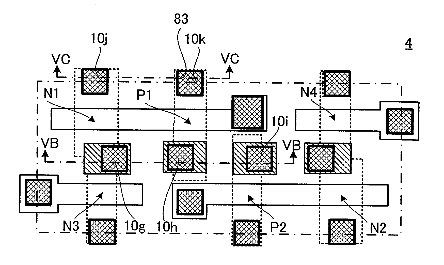
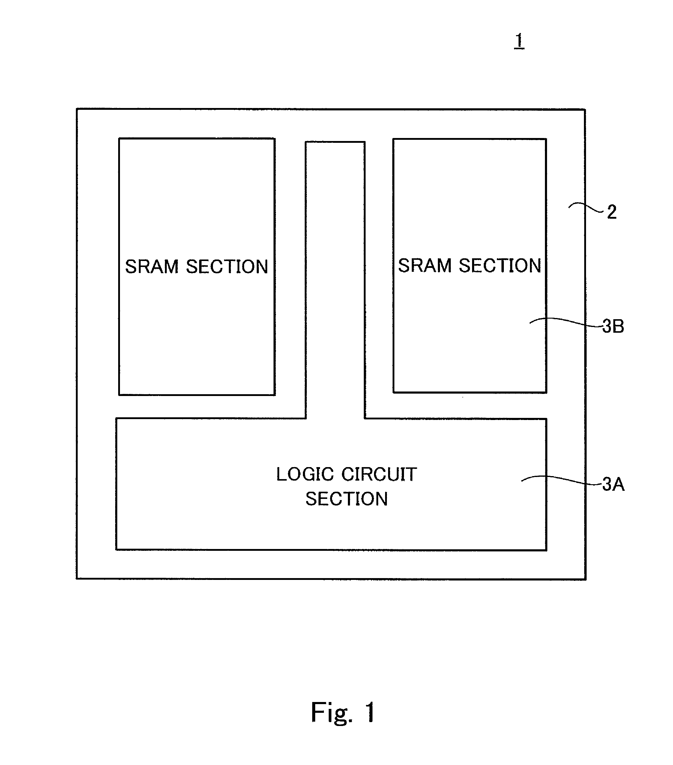
[0070]FIG. 1 shows an example of a block diagram of a semiconductor device according to a first exemplary embodiment of the present invention. As shown in FIG. 1, a semiconductor device 1 according to the first exemplary embodiment is a so-called SoC (System on a Chip) device including a logic circuit section 3A and two SRAM sections 3B each serving as a memory section. The logic circuit section 3A and the two SRAM sections 3B are formed on a semiconductor substrate 2. Each of the SRAM sections 3B includes a memory cell region, a decoder region, and a memory control circuit region. In the memory cell region, a plurality of memory cells 4 is arranged in a matrix. In the first exemplary embodiment, the memory cells 4 correspond to a regular layout region. The logic circuit section corresponds to an irregular layout region.

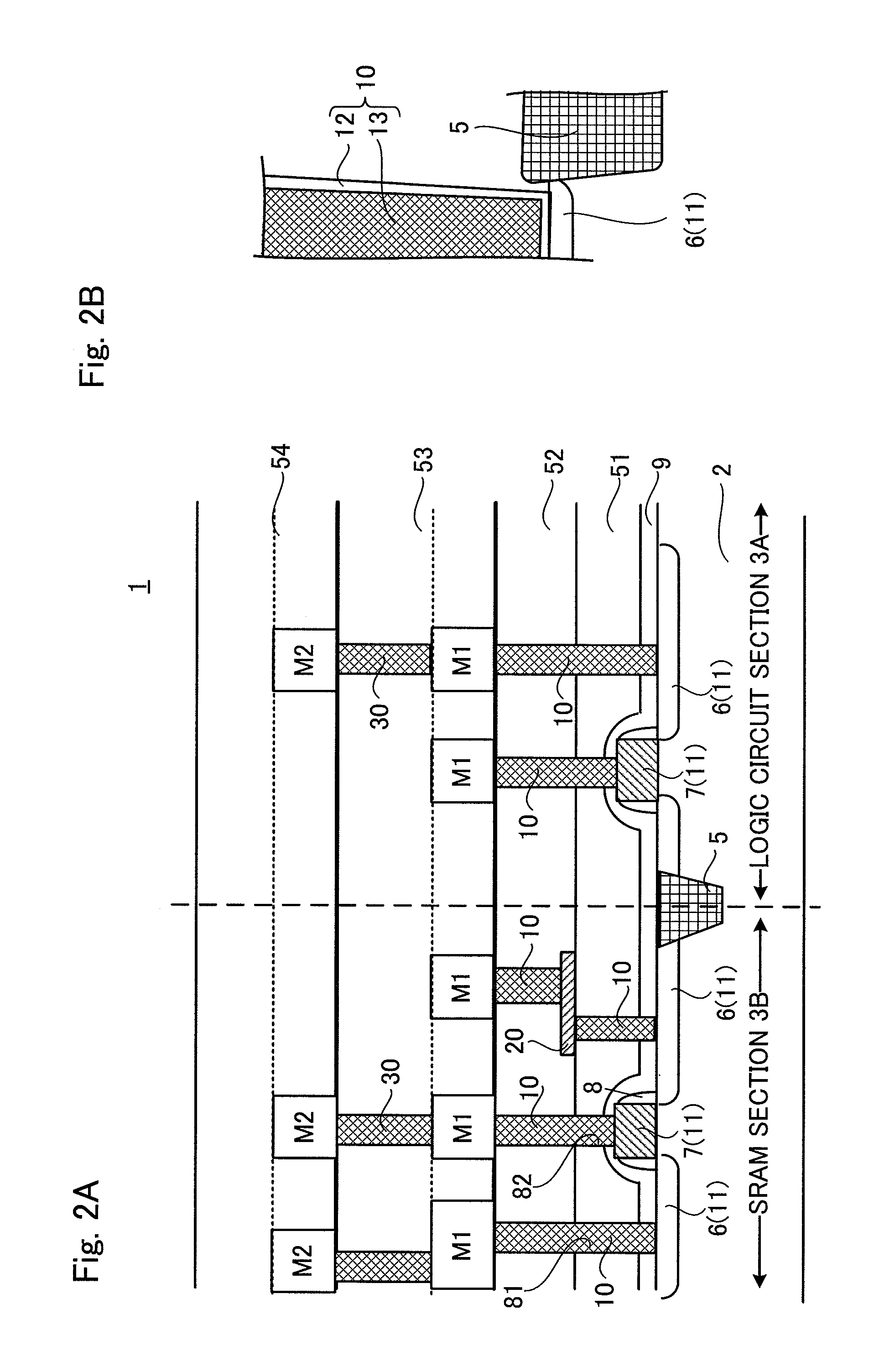
[0071]FIG. 2A shows a partial sectional view schematically showing the SRAM section 3B and the logic circuit section 3A of the semiconductor device 1 according to th...

second exemplary embodiment

[0094]Next, a description is given of an exemplary embodiment of a semiconductor device which is different from the above-mentioned exemplary embodiment. Note that components identical with those of the above-mentioned exemplary embodiment are denoted by the same reference symbols, and the description thereof is omitted as appropriate.

[0095]The basis structure of a semiconductor device according to a second exemplary embodiment of the present invention is similar to that of the first exemplary embodiment, except for the following. That is, in the semiconductor device 1 according to the first exemplary embodiment, the connection holes 81 and 82 are formed at the positions where the intermediate connection layer 20 is not formed, after the formation of the first interlayer insulating film 51, and the M1-connection plugs 10 (e.g., 10a to 10f) are disposed. Then, after the formation of the second interlayer insulating film 52, the connection holes 83 are formed and the M1-connection plu...

third exemplary embodiment

[0101]The basic structure of a semiconductor device according to a third exemplary embodiment of the present invention is similar to that of the first exemplary embodiment, except for the following. That is, in the semiconductor device 1 according to the first exemplary embodiment, the intermediate connection layer 20 is formed only in the region in which the arrangement positions of the M1-connection plugs 10 are intended to be shifted from the immediately above positions extending from immediately above the lower conductive layer 11. Meanwhile, in the semiconductor device according to the third exemplary embodiment, the intermediate connection layer 20 is formed at all the positions where the M1-connection plugs 10 are disposed in a gap between the first interlayer insulating film 51 and the second interlayer insulating film 52.

[0102]Reference is now made to FIG. 9 which is a partial sectional view schematically showing the SRAM section 3B and the logic circuit section 3A of a sem...


PUM


Abstract

An exemplary embodiment of the present invention is a semiconductor device having a regular layout region and an irregular layout region formed on one chip, including: a lower conductive layer; an interlayer insulating film formed on the lower conductive layer; an upper interconnect layer formed on the interlayer insulating film; and connection plugs disposed to electrically connect the lower conductive layer and the upper interconnect layer at a substantially shortest distance. In at least part of the regular layout region, the lower conductive layer and the upper interconnect layer are electrically connected to each other through at least two connection plugs and an intermediate connection layer for electrically connecting the at least two connection plugs, the at least two connection plugs being disposed at an immediately above position extending from immediately above the lower conductive layer and a shift position spaced apart from the immediately above position, respectively.

Description

BACKGROUND[0001]1. Field of the Invention[0002]The present invention relates to a semiconductor device, and more particularly, to a semiconductor device including a regular layout region.[0003]2. Description of Related Art[0004]As basic structures of SRAM (Static Random Access Memory) memory cells for use in semiconductor memory devices, there are known a high-resistance load type SRAM including four MOS (Metal Oxide Semiconductor) transistors (two drive MOS transistors and two transfer MOS transistors) and two high-resistance elements, and a CMOS (Complementary Metal Oxide Semiconductor) type SRAM including six MOS transistors (two drive MOS transistors, two load MOS transistors, and two transfer MOS transistors) (e.g., see U.S. Pat. Nos. 5,930,163, 6,900,513, 6,597,041, and 6,922,354). Along with the recent tendency toward the reduction in voltage due to the miniaturization of design rules, CMOS-type SRAMs are widely employed as semiconductor memory devices which are mixed in a lo...

Claims


Application Information

Patent Timeline
Patent Type & Authority Patents(United States)
IPC IPC(8): H01L23/48H01L23/52H01L29/40
CPCH01L27/0207H01L27/105H01L27/1104H01L27/1116Y10S257/903H01L2924/0002H01L2924/00H10B10/18H10B10/12
Inventor OOKA, HIDEYUKI
Owner RENESAS ELECTRONICS CORP
Why Eureka
Try Eureka