Vapor-phase epitaxial growth method and vapor-phase epitaxy apparatus

a growth method and epitaxy technology, applied in the direction of polycrystalline material growth, crystal growth process, chemically reactive gas, etc., can solve the problems of tight contact, uneven film thickness, and reduced production yield of semiconductor integrated circuit chips per wafer

Inactive Publication Date: 2011-08-30
NUFLARE TECH INC
View PDF15 Cites 7 Cited by
  • Summary
  • Abstract
  • Description
  • Claims
  • Application Information

AI Technical Summary

Benefits of technology

[0010]It is therefore an object of this invention to provide an improved vapor-phase epitaxy (VPE) technique capable of uniformizing the thickness of an epitaxially grown semiconductor layer or film while appropriately controlling epitaxial growth conditions.

Problems solved by technology

This results in tight contact or “adhesion,” which leads to occurrence of a program that the Si wafer 500 is rigidly adhered to the holder 510 accidentally during conveyance of this wafer.
Unfortunately, even with the use of the above-stated approaches, the silicon epitaxial film as grown at peripheral surface portions of the silicon wafer 500 can become thinner, resulting in the film thickness being made irregular to loose the uniformity.
This appreciably reduces the production yield of semiconductor integrated circuit chips per wafer.

Method used


Image

  • Vapor-phase epitaxial growth method and vapor-phase epitaxy apparatus
  • Vapor-phase epitaxial growth method and vapor-phase epitaxy apparatus
  • Vapor-phase epitaxial growth method and vapor-phase epitaxy apparatus

Examples


embodiment 1

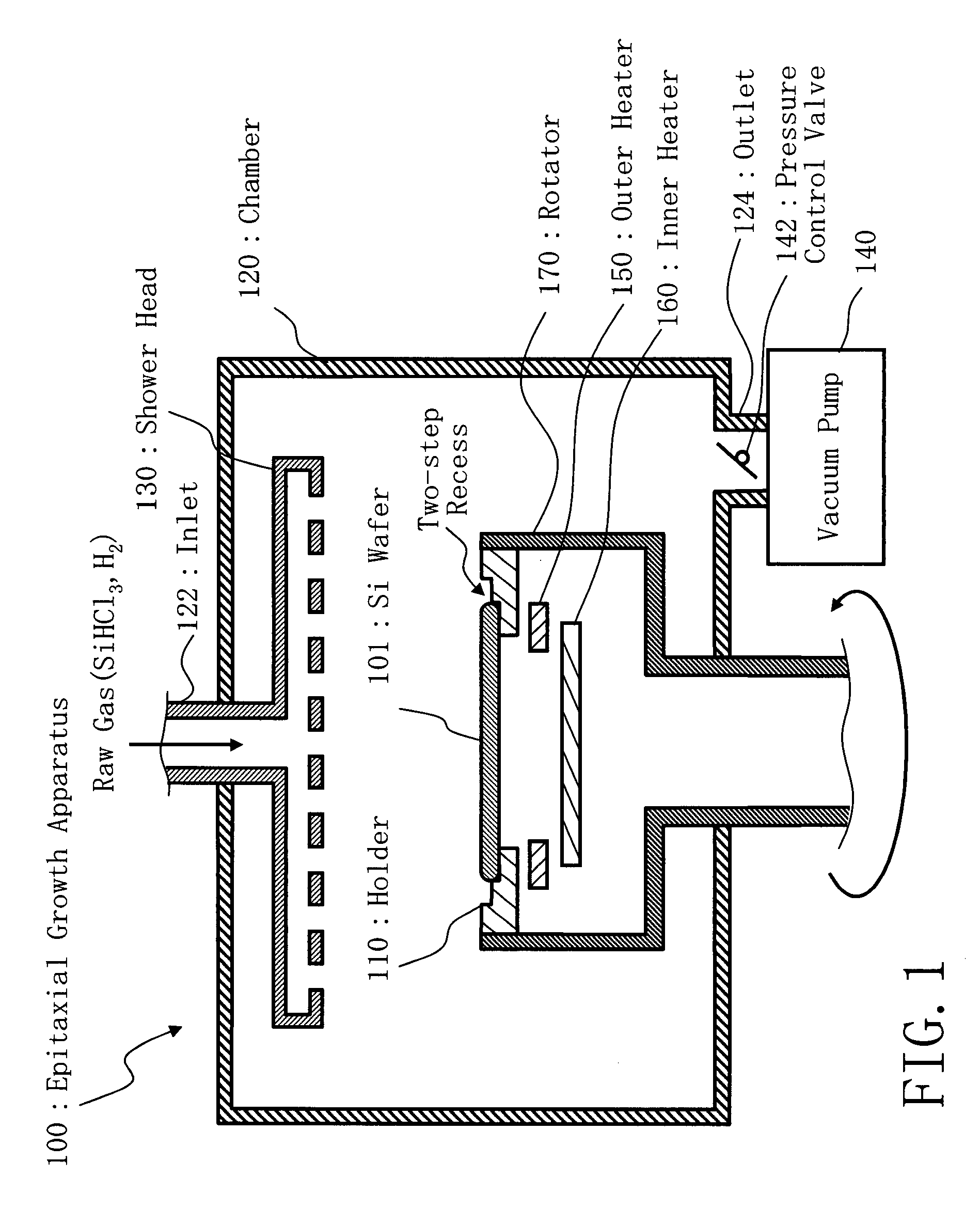
[0053]A vapor-phase epitaxy (VPE) apparatus 100 embodying this invention is shown in FIG. 1 with respect to main part thereof. As shown herein, this VPE tool 100 is generally made up of a workpiece support structure 110, also known as holder or susceptor, in the interior space of an epitaxial growth reactor chamber 120. This chamber 120 has a shower head 130, a vacuum pump 140, a gas pressure control valve 142, an outer heater 150, an inner heater 160, and a rotating member 170. The chamber 120 is associated with a gas inflow path 122 and a gas outflow path 124 which are coupled thereto. The gas inlet 122 is coupled to the shower head 130. Note that the illustration here is not to scale for purposes of convenience in illustration. The same goes with respective ones of the other drawings.

[0054]The holder 110 is circular in its outer circumference with a through-going opening of a prespecified inside diameter being formed therein. Holder 110 also has a circular recess, or “depressed p...

embodiment 2

[0075]Turning to FIG. 9, a top plan view of a wafer holder 110 in accordance with another embodiment of this invention is shown in the state that a silicon wafer 101 is mounted and supported thereby. A sectional view of the holder 110 is depicted in FIG. 10. In this embodiment, an annular array of multiple upstanding pins 112 is disposed as an alternative to the forming of the internal recess 114 shown in FIG. 4. VPE process conditions are similar to those of the previous embodiment. As shown in FIG. 9, the holder 110 has a circular recess 116, or “depressed portion 116” corresponding to the outer large-diameter recess of FIG. 4. This “second” recess 116 is slightly larger in diameter than the Si wafer 101 and has a depth that is less than one-half of the thickness of Si wafer 101. Holder 110 also has a through-hole at the center of a bottom surface of recess 116, which hole is less in diameter than wafer 101. Si wafer 101 is mounted and supported on an annular bottom surface of the...

embodiment 3

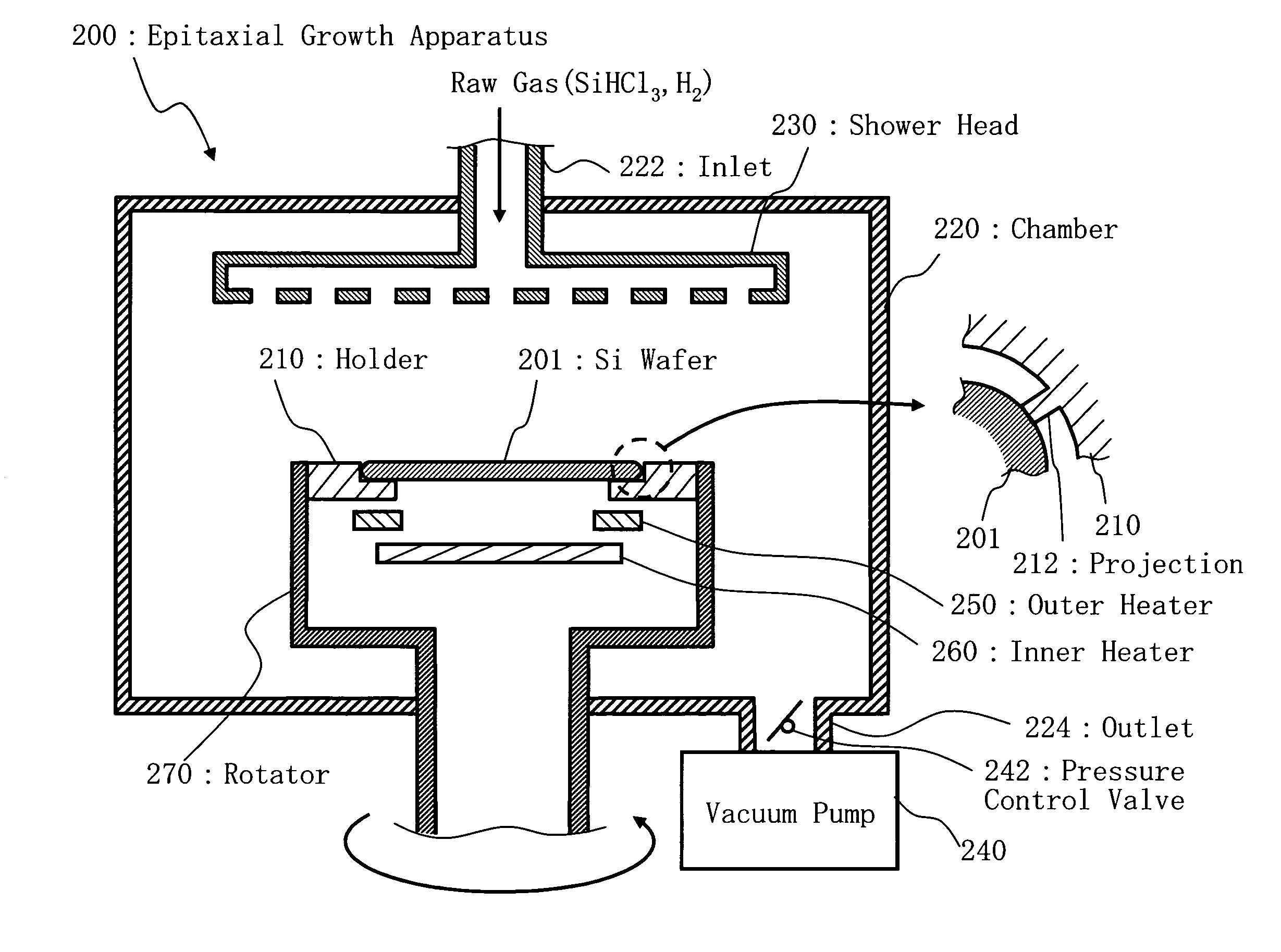
[0078]A vapor-phase epitaxy (VPE) apparatus 200 also embodying this invention is shown in FIG. 11. As in the embodiment of FIG. 1, this VPE tool 100 includes a substrate support holder 210, also known as susceptor, in the interior space of a growth reactor chamber 220. This chamber 220 has a shower head 230, a vacuum pump 240, a gas pressure control valve 242, an outer heater 250, an inner heater 260, and a rotating member 270. The chamber 220 is associated with a gas inflow path 222 and a gas outflow path 224 which are coupled thereto. The gas inlet 222 is coupled to the showerhead 230.

[0079]The holder 210 has a circular shape in its outer circumference, with a through-hole of a predetermined internal diameter being centrally formed therein—i.e., it is a hollow ring-like plate with a center hole. The holder 210 has in the hole a recess, or “depressed portion” with an annular flat bottom surface at a mid level or “depth” from the top surface of holder 210, and supports a semiconduct...


PUM

PropertyMeasurementUnit
temperatureaaaaaaaaaa
internal pressureaaaaaaaaaa
atmospheric pressureaaaaaaaaaa

Abstract

A vapor phase epitaxial growth method using a vapor phase epitaxy apparatus having a chamber, a support structure holding thereon a substrate in the chamber, a first flow path supplying a reactant gas for film formation on the substrate and a second flow path for exhaust of the gas, said method includes rotating the substrate, supplying the reactant gas and a carrier gas to thereby perform vapor-phase epitaxial growth of a semiconductor film on the substrate, and during the vapor-phase epitaxial growth of the semiconductor film on the substrate, controlling process parameters to make said semiconductor film uniform in thickness, said process parameters including flow rates and concentrations of the reactant gas and the carrier gas, a degree of vacuum within said chamber, a temperature of the substrate, and a rotation speed of said substrate.

Description

CROSS-REFERENCE TO RELATED APPLICATION(S)[0001]Priority is claimed to Japanese Patent Application (JPA) No. 2006-075894, filed Mar. 20, 2006, the disclosure of which is incorporated herein by reference.FIELD OF THE INVENTION[0002]The present invention relates generally to vapor-phase epitaxy (VPE) technologies and, more particularly, to a method and apparatus for forming an epitaxial film grown on a wafer or substrate with controlled growth conditions. This invention also relates to a wafer holder structure adaptable for use in the VPE apparatus.DESCRIPTION OF RELATED ART[0003]Single-crystal epitaxy techniques with well controlled impurity concentration and film thickness is becoming important more and more in the manufacture of advanced semiconductor devices of enhanced performance, such as ultrahigh-speed bipolar and complementary metal oxide semiconductor (CMOS) transistors.[0004]Epitaxy is typically a process to grow a single-crystalline layer or film on a semiconductive substra...

Claims


Application Information

Patent Timeline
Patent Type & Authority Patents(United States)
IPC IPC(8): C30B21/04
CPCC23C16/4584C23C16/4585C23C16/4586C30B25/12C30B25/165H01L21/02661H01L21/68728H01L21/68735H01L21/02381H01L21/02532H01L21/0262C30B29/06
Inventor ITO, HIDEKIINADA, SATOSHIMORIYAMA, YOSHIKAZU
Owner NUFLARE TECH INC
Why Eureka
Try Eureka