Latency signal generating circuit and semconductor device having the same

a technology of generating circuit and semconductor, applied in pulse generators, pulse techniques, instruments, etc., can solve the disadvantages of increasing the chip size of the semiconductor device, the increase of the cas latency cl, and the semiconductor device's semiconductor device's disadvantages, so as to minimize the power consumption of generating a dll clock signal and high speed operation.

Inactive Publication Date: 2011-10-04
SK HYNIX INC
View PDF11 Cites 53 Cited by
  • Summary
  • Abstract
  • Description
  • Claims
  • Application Information

AI Technical Summary

Benefits of technology

[0037]Conventionally, it is required to modify the design of a counter circuit and a comparator circuit according to CAS latency. It caused many problems. However, the latency signal generating circuit according to the present invention can generate a latency signal corresponding CAS latency without designing a counter circuit and a comparator circuit. Therefore, the latency signal generating circuit according to the present invention is suitable to a development direction of a semiconductor device for high speed operation, low power consumption, and miniaturization. Also, the delay locked loop according to the present invention is enabled for desired periods. Therefore, it is possible to minimize power consumption for generating a DLL clock signal.

Problems solved by technology

However, such a semiconductor device may have the following problems.
At first, the increment of an operation frequency of a semiconductor device causes increasing CAS latency CL.
That is, a chip size of a semiconductor device disadvantageously increases.
Also, since a 4-bit counter circuit has a slower operation speed than that of a 3-bit counter circuit, the operation speed of the counter circuit become slow as the CAS latency CL increases.
Then, an operation speed of the comparing circuit becomes slow as the number of bits increases.
That is, a data processing speed of a semiconductor device becomes slow.
It means a semiconductor device may waste power until the read command RD is applied.
Thus, the delay locked loop DLL circuit may waste power continuously.

Method used


Image

  • Latency signal generating circuit and semconductor device having the same
  • Latency signal generating circuit and semconductor device having the same
  • Latency signal generating circuit and semconductor device having the same

Examples


Embodiment Construction

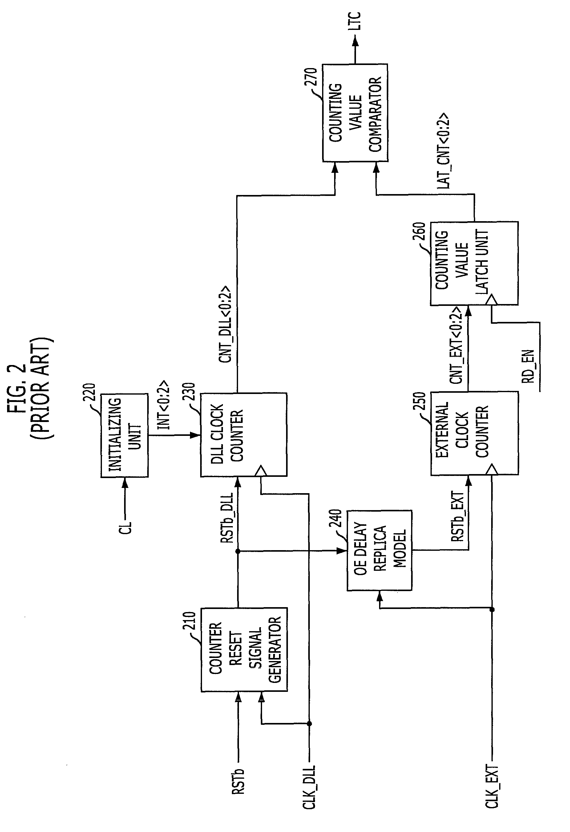
m showing an operation timing of a locking completion signal synchronizer 530 of FIG. 5.

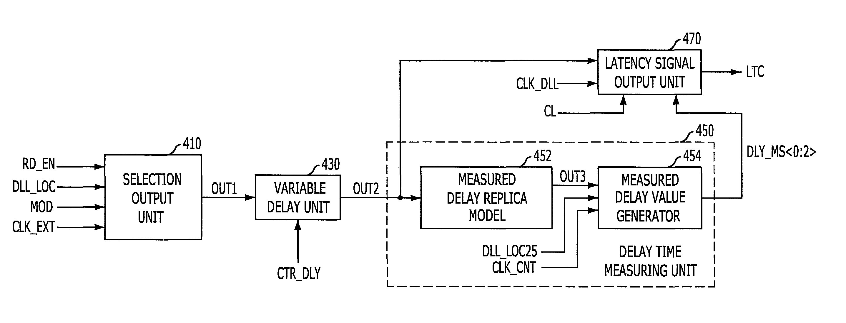
[0045]FIG. 8 is a diagram illustrating a measured delay value generator 454 of FIG. 4.

[0046]FIG. 9 is a waveform showing an operation timing of a measured delay value generator 454 of FIG. 8.

[0047]FIG. 10 is a diagram illustrating a latency signal output unit 470 of FIG. 4.

[0048]FIG. 11 is a waveform showing an operation timing of a plurality of shifters 1030 of FIG. 10.

[0049]FIGS. 12A and 12B are waveforms showing an operation of a latency signal generating circuit in accordance with an embodiment of the present invention.

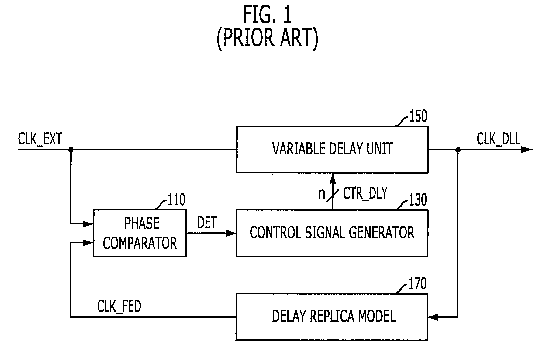
[0050]FIG. 13 is a block diagram illustrating a circuit for generating a DLL clock signal CLK_DLL.

[0051]FIGS. 14 to 16 are diagrams showing an input controller 1310 of FIG. 13 according to various embodiments.

[0052]FIG. 17 illustrates a block diagram generating a control signal of a variable delay unit 430 of FIG. 4.

DESCRIPTION OF SPECIFIC EMBODIMENTS

[0053]Hereinafter, a regist...


PUM


Abstract

A semiconductor device includes a latency signal generating circuit for generating a latency signal corresponding CAS latency by measuring a delay amount reflected at a delay locked loop and reflecting the measured delay amount at a read command signal, and a delay locked loop for controlling an internal clock signal applied to the latency signal generating circuit corresponding to the read command and the latency signal. The semiconductor device includes an internal clock signal generating block configured to generate an internal clock signal, a latency generating block configured to generate a latency signal by synchronizing a read command signal with the internal clock signal at a time corresponding to a CAS latency value and a measured delay value, and an input controlling block configured to activate the reference clock signal using an external clock signal in response to the read command signal and the latency signal.

Description

CROSS-REFERENCE TO RELATED APPLICATIONS[0001]The present invention claims priority of Korean patent application number 10-2008-0137382, filed on Dec. 30, 2008, the disclosure of which is incorporated herein by reference in its entirety.BACKGROUND OF THE INVENTION[0002]The present invention relates to semiconductor design, and more particularly, to a latency signal generating circuit for outputting a latency signal by synchronizing a read command signal, which is synchronized with an external clock signal, with an internal clock signal, and an internal clock signal generating circuit for outputting an internal clock signal by compensating an received external clock signal for an internal delay time of a semiconductor device.[0003]In general, a semiconductor device such as a Double Data Rate Synchronous DRAM (DDR SDRAM) receives an external clock signal, generates an internal clock signal based on the received external clock signal, and uses the generated internal clock signal as a re...

Claims


Application Information

Patent Timeline
Patent Type & Authority Patents(United States)
IPC IPC(8): H03H11/26
CPCG11C7/1045G11C7/1087G11C7/1093G11C7/22G11C7/222G11C11/4076H03L7/0814G11C2207/2272H03L7/0816
Inventor KIM, KYUNG-HOON
Owner SK HYNIX INC
Why Eureka
Try Eureka