Color conversion type organic EL display

a technology of organic display and color conversion, applied in the direction of instruments, discharge tubes, luminescent screens, etc., can solve the problems of reducing the absorbance of light to be absorbed, affecting the efficiency of organic display, etc., to achieve the effect of long life and high efficiency

Active Publication Date: 2011-10-25
SHARP KK
View PDF29 Cites 21 Cited by
  • Summary
  • Abstract
  • Description
  • Claims
  • Application Information

AI Technical Summary

Benefits of technology

[0018]An object of this invention is to provide a color conversion type organic EL display, which performs multicolor emission with high efficiency and a long lifetime through the selective fine formation of a color conversion layer above an emission layer, without using metal masks which pose problems for resolution or expensive laser scanning devices.
[0020]By means of the this invention adopting the configuration described above, a structure is employed in which an organic polymer EL material is used to form an emission layer divided by a bank held between a lower reflective electrode and an upper transparent electrode, a color conversion layer is formed directly on the upper transparent electrode, and moreover bonding is performed with a separate substrate on which a color filter and black matrix are formed, so that the following advantageous results are obtained.
[0021](1) Normal photo processes can be used to accurately control film thickness, to form a color filter on a transparent substrate, so that variation in chromaticity can be held to a minimum.
[0022](2) A color conversion layer is formed directly on an organic EL device, so that EL light is incident on the color conversion layer without loss, and a highly efficient organic EL display can be realized.

Problems solved by technology

It has been reported that in such devices, the balance of emission intensities among emissive materials changes with the passage of time during driving or with the current passed, and that there are concerns that the hues obtained may change.
Here, if the concentration of the color conversion material is lowered, the absorbance of the light to be absorbed is reduced, and adequate converted light intensity cannot be obtained.
When using such a thick color conversion film (film thickness approximately 10 μm), such problems as disconnection of electrode patterns at step portions, difficulty in increasing definition, and residual water or solvent in the film (when combined with an organic EL device, residual water or solvent causes alteration of the organic EL layer, resulting in display faults) exist.
On the other hand, from the standpoint of reducing viewing angle dependence, there is also a conflicting demand for a thinner color conversion film.
However, when forming a color conversion film using an evaporation deposition method, if the film is formed over the entirety of the display face, division into three primary colors to cause emission is not possible, and so some means for forming a fine pattern corresponding to specific pixels becomes necessary.
However, due to limits on the mask material and thickness, the fineness of the pattern of the metal mask used has a limit of a definition level of 150 ppi.
Application of selective application methods using metal masks to patterns with definitions higher than this entail such problems as increased difficulty, extreme difficulty when increasing the area, and reduced yields.
However, in the above method, there are the problems that the efficiency of material utilization of expensive color conversion material is poor, and moreover that the color conversion performance is degraded by direct polishing of the color conversion layer.
This gap causes the problems of crosstalk phenomena in which light from the EL device leaks into adjacent pixels, and of the phenomenon of losses due to inadequate incidence of light from the EL device onto the color conversion layer.
Consequently it is difficult to adequately remove from the color filter and color conversion layer the moisture and solvents which exert the most adverse effects on the organic EL material, and these can easily be imagined to critically degrade the device lifetime.

Method used


Image

  • Color conversion type organic EL display
  • Color conversion type organic EL display

Examples


first embodiment

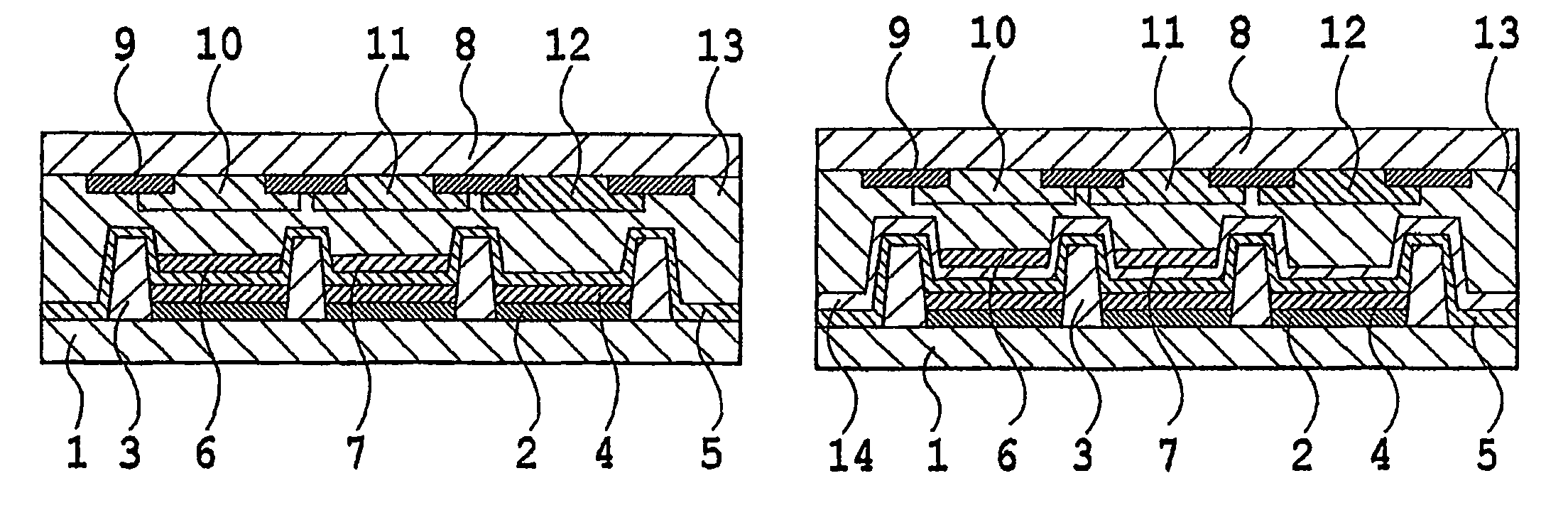
[0027]FIG. 1 is a summary cross-sectional view of the color conversion type organic EL display of a first embodiment of the invention.

[0028](TFT Substrate 1)

[0029]The TFT substrate 1 is a substrate on which is formed a TFT circuit comprising the organic EL display. The uppermost surface of the TFT substrate 1 is covered with an insulating planarization layer, and contact electrodes connected with the TFT circuit, divided into pixel units, are formed. Thereupon is formed a lower reflective electrode, joined with TFTs by contact electrodes, serving as cathodes or as anodes, and separated into pixel units.

[0030]The substrate material may be any insulating material; glass is primarily used, but a polymer material, ceramic, or Si single crystal may also be used without problem.

[0031](Lower Reflective Electrode 2)

[0032]In order to form a top-emission structure organic EL device, a light-reflecting material must be used in the lower reflective electrode 2. Light-reflecting metals which can...

second embodiment

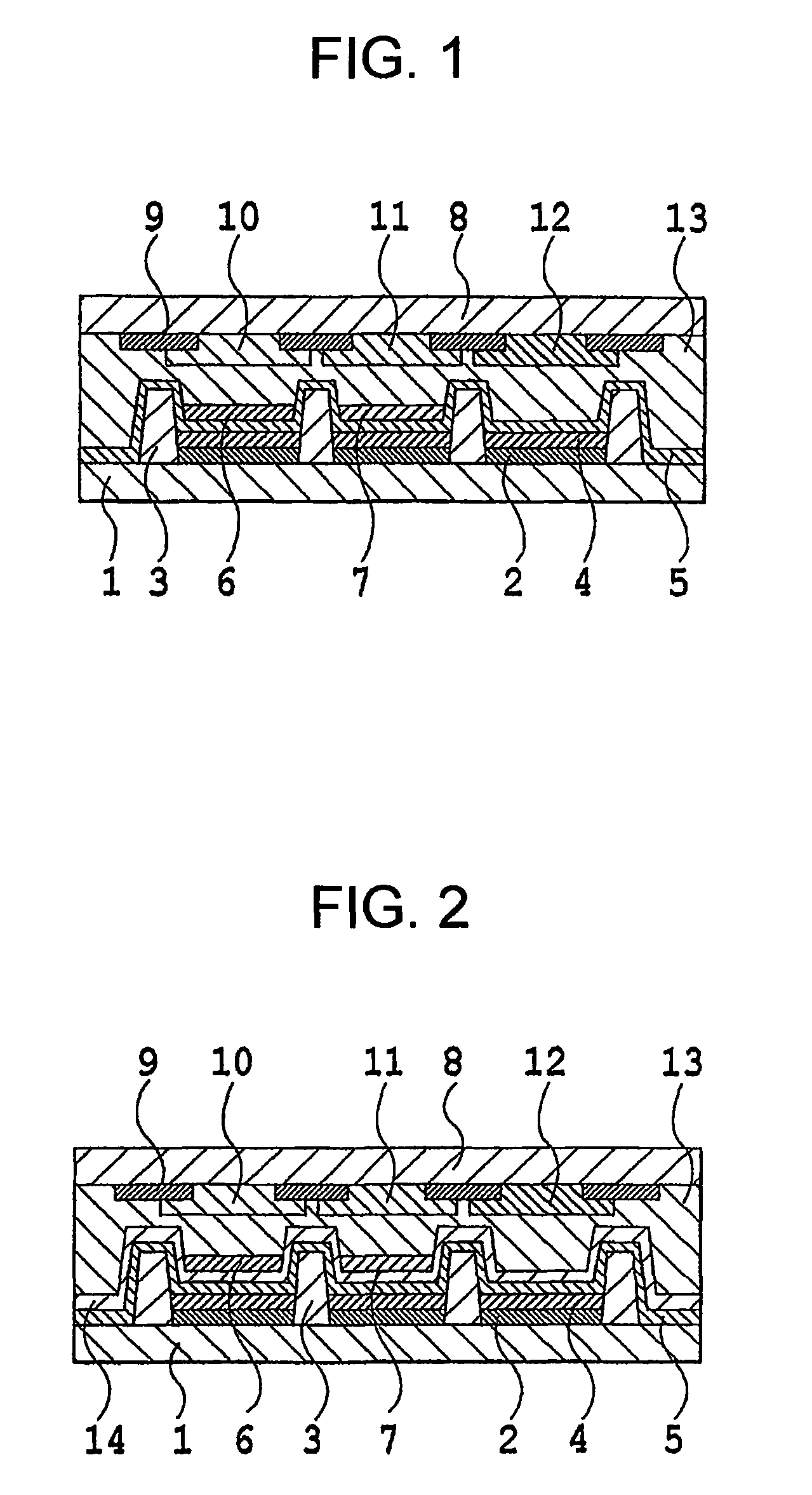
[0066]FIG. 2 is a summary cross-sectional view of the color conversion type organic EL display of a second embodiment of the invention. The color conversion type organic EL display of the second embodiment of the invention has a configuration similar to that of the first embodiment, except for the existence of a transparent protective layer 14 on the upper transparent electrode 5, and the fact that the color conversion layers (6, 7) are formed on the transparent protective layer 14.

[0067](Transparent Protective Layer 14)

[0068]The color conversion layers (6, 7) may be formed directly on the upper transparent electrode 5, but when the method of formation of the color conversion layers (6, 7) is a wet method, if there are pinholes in the upper transparent electrode 5, then intrusion of solvent into the organic EL layer 4 (and in particular the emission layer) is conceivable, and so a transparent protective layer 14 can be inserted on the upper transparent electrode 5.

[0069]As the mater...

example 1

[0070]This example is an example of the first embodiment of the invention. In this example, a substrate which was an alkali-free glass sheet of thickness 0.7 mm, on which was formed a circuit using amorphous Si-TFTs, was used as the TFT substrate 1.

[0071]On the TFT substrate 1, an evaporation deposition method was used to form an Al film of film thickness 100 nm, and a photolithography process was used to perform patterning into pixel region shapes. Specifically, a plurality of partial electrodes, having dimensions 300 μm×100 μm, were formed from the Al film. The gaps between the partial electrodes were 30 μm in the vertical direction and 10 μm in the horizontal direction. Partial electrodes were arranged with 50 in the vertical direction and 150 in the horizontal direction.

[0072]Next, after applying VPA100P5.0, manufactured by Nippon Steel Chemical Co., Ltd., a photolithography method was used to perform patterning, and a bank was formed in the gaps (in the vertical direction and h...


PUM

PropertyMeasurementUnit
thicknessaaaaaaaaaa
thicknessaaaaaaaaaa
temperatureaaaaaaaaaa

Abstract

A color conversion type organic EL display can comprise an organic EL substrate that includes a substrate, a lower reflective electrode, a bank, and an organic EL layer sandwiched between the lower reflective electrode and an upper transparent electrode. The color conversion type organic EL display can further comprise a color filter substrate in which a black matrix and a color filter are formed in a pattern on a transparent substrate by a photo process, and which has a pixel region separated by the black matrix. The organic EL substrate and the color filter substrate can be bonded together and positioned such that the pixel region of the EL substrate and the pixel region of the color filter substrate are opposed.

Description

CROSS-REFERENCE TO RELATED APPLICATIONS[0001]This application is a national stage application under 35 U.S.C. §371 of International Application No. PCT / JP2009 / 063186, filed Jul. 23, 2009, and claims the benefit under 35 U.S.C. §119 of the earlier filing date of Japanese Patent Application 2008-195154, filed Jul. 29, 2008. International Application No. PCT / JP2009 / 063186 and Japanese Patent Application 2008-195154 are hereby incorporated herein in their entirety by reference.TECHNICAL FIELD[0002]This invention relates to a device structure of an organic display, in which full-color display is achieved by forming a color conversion film directly on a top-emission type organic EL device.BACKGROUND ART[0003]In recent years, active research aimed at commercialization of organic EL devices has been conducted. Organic EL devices can achieve high current densities at low voltages, and so are expected to make possible high emission brightnesses and high emission efficiencies, and in particula...

Claims


Application Information

Patent Timeline
Patent Type & Authority Patents(United States)
IPC IPC(8): H01J1/62
CPCH01L27/322Y10T29/49117H01L2251/5315H10K59/38H10K2102/3026G02B5/201H10K50/814H10K50/818H10K50/828H10K50/844
Inventor KAWAMURA, YUKINORI
Owner SHARP KK
Why Eureka
Try Eureka