Dual sensitivity image sensor

a dual-sensitivity, image sensor technology, applied in the field of cmos image sensors, can solve the problems of increasing sensor noise, degrading the dynamic range of video applications or exposure latitude for still capture, and increasing the noise-based iso speed, so as to effectively replace the capacitance of pixel sense, increase pixel complexity, and enhance sensitivity

Active Publication Date: 2011-11-22
SAMSUNG ELECTRONICS CO LTD
View PDF18 Cites 15 Cited by
  • Summary
  • Abstract
  • Description
  • Claims
  • Application Information

AI Technical Summary

Benefits of technology

[0011]The present invention is a programmable pixel circuit for iSoC image sensors that supports two modes of operation to alternately deliver nominal or enhanced sensitivity. Dual-mode operation is achieved by supporting multi-mode pixel operation via system-on-chip functionality in peripheral circuits supporting pixel readout from the embedded imaging matrix array. There is consequently no significant increase in pixel complexity or degradation in optical fill factor. The low-noise, high-sensitivity mode is achieved by effectively replacing the pixel sense capacitance with the smaller capacitance of a switched capacitor integrator that is built using the same transistors as the source follower amplifier of the standard configuration.
[0013]A column buffer circuit is additionally connected to the signal bus and the dual sensitivity selection and support circuit and the column buffer are shared by a column of pixels in an image sensor. In a preferred embodiment, the amplifier transistor and the readout transistor are formed as a single dual-gate transistor to reduce the Miller capacitance associated with the circuit.

Problems solved by technology

This approach typically degrades dynamic range for video applications or exposure latitude for still capture use.
Post-pixel amplification also raises the requisite gain-bandwidth requirement for the signal processing chain and thereby often increases sensor noise.
Consequently, while the sensitivity-based ISO speed is set higher, the noise-based ISO speed often actually degrades.
Unfortunately, particularly under condition of the higher gain settings and for high frame rate applications such as high definition television, the requisite gain-bandwidth product of the amplifier stages can be especially challenging to support and thereby generate nonlinearity, excess noise, or other artifacts.
Furthermore, generation of excess white noise is likely since gain is applied after signal is transferred to the column buffer.

Method used


Image

  • Dual sensitivity image sensor
  • Dual sensitivity image sensor
  • Dual sensitivity image sensor

Examples


Embodiment Construction

[0023]The following description is provided to enable any person skilled in the art to make and use the invention and sets forth the best modes contemplated by the inventor for carrying out the invention. Various modifications, however, will remain readily apparent to those skilled in the art. Any and all such modifications, equivalents and alternatives are intended to fall within the spirit and scope of the present invention.

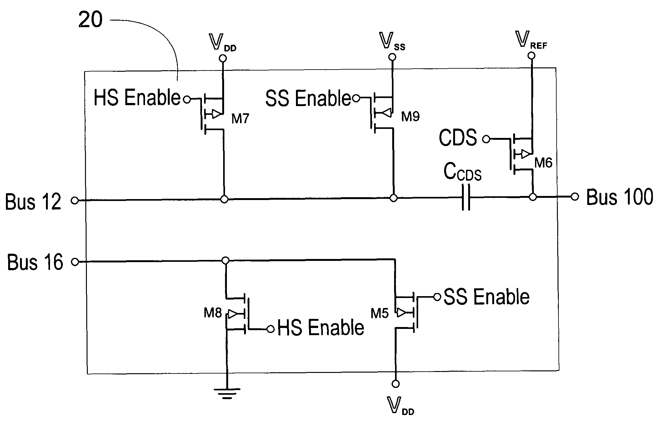
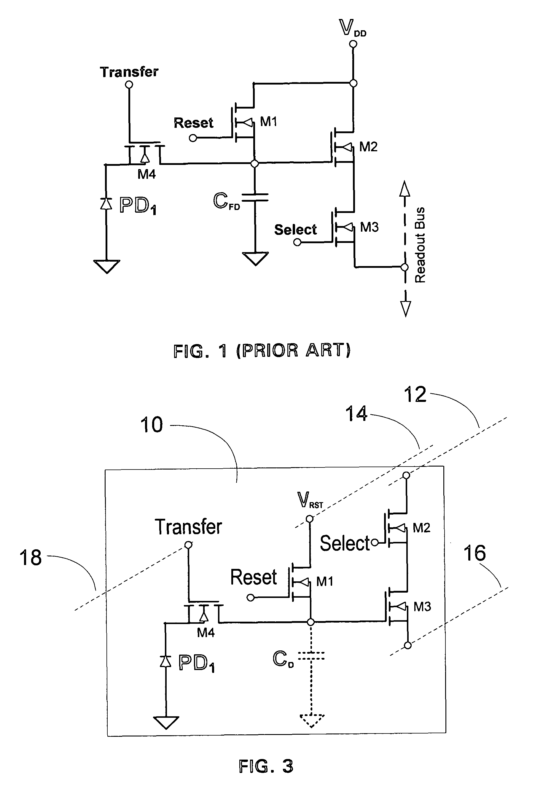
[0024]According to the present invention, an imaging System-on-Chip (iSoC) circuit supporting dual-mode sensitivity is provided that comprises few transistors and bias supplies per pixel and maintains high optical fill factor, low noise and compatibility with conventional CMOS image sensor (CIS) process technology. The two sensitivity modes include: 1) a standard mode featuring nominal sensitivity and noise for most lighting conditions and; 2) an enhanced sensitivity mode for operation at low light levels with lower temporal noise. In addition, the enhanced sen...


PUM


Abstract

A dual sensitivity image sensor provides a standard mode and a high-sensitivity mode of operation via iSoC integration. In addition to boosting sensitivity, the high sensitivity mode also reduces temporal noise thereby optimally boosting the Signal-to-Noise Ratio (SNR) of the image sensor. The circuit does not significantly increase pixel complexity and requires minimal changes to the support circuits in the iSoC including the addition of support and control circuitry to facilitate seamless mode change.

Description

BACKGROUND OF THE INVENTION[0001]1. Field of the Invention[0002]The present invention relates generally to CMOS image sensors, and more particularly to pixel circuits for imaging System-on-Chip (iSoC) sensors capable of imaging under a variety of lighting conditions including low light.[0003]2. Description of the Related Art[0004]Visible imaging systems implemented using CMOS image sensors significantly reduce camera cost and power while improving resolution and reducing noise. The latest cameras use CMOS iSoC sensors that efficiently marry low-noise image detection and processing with a host of supporting blocks including timing controller, clock drivers, reference voltages, A / D conversion and key signal processing elements. High-performance video cameras are now produced using a single CMOS integrated circuit supported by only a lens and battery. These improvements translate into smaller camera size and longer battery life. The improvements also translate to dual-use cameras that ...

Claims


Application Information

Patent Timeline
Patent Type & Authority Patents(United States)
IPC IPC(8): H04N3/14H04N5/335H04N5/343H04N5/357H04N5/369
CPCH04N5/23245H04N5/3575H04N5/363H04N5/3742H04N5/378H01L27/14643H04N23/667H04N25/616H04N25/65H04N25/767H04N25/75
Inventor KOZLOWSKI, LESTER J.
Owner SAMSUNG ELECTRONICS CO LTD
Why Eureka
Try Eureka