Semiconductor device and method for manufacturing the same

a semiconductor and semiconductor technology, applied in the field of semiconductor devices, can solve the problems of silicon semiconductors not suitable for use in such severe environments, power devices are sometimes required to operate in severe environments, and the performance of silicon power devices is now approaching the theoretical limit, so as to prevent graphite deposition, prevent the adhesiveness between the ohmic electrode and the pad electrode from being decreased, and prevent the effect of contact resistan

Active Publication Date: 2011-12-13
PANASONIC CORP
View PDF17 Cites 3 Cited by
  • Summary
  • Abstract
  • Description
  • Claims
  • Application Information

AI Technical Summary

Benefits of technology

In a semiconductor device according to the present invention, the ohmic electrode contains an alloy of titanium, silicon and carbon, and the gate electrode contains titanium silicide. Therefore, in the ohmic electrode, deposition of graphite is prevented when the ohmic contact is formed. This prevents the contact resistance from being increased and also prevents the adhesiveness between the ohmic electrode and the pad electrode from being decreased, and thus deterioration of the reliability can be prevented. In the gate electrode, the formation of titanium silicide can decrease the gate resistance. As a result, the characteristics of the semiconductor device can be improved. In addition, it is possible to form the gate electrode and the ohmic electrode in the same process. This can reduce the production cost and the time required for the production and also can improve the yield.

Problems solved by technology

However, the performance of the silicon power devices is now approaching the theoretical limit thereof.
In addition, power devices are occasionally required to operate in severe environments, for example, at a high temperature or under radiation.
Silicon semiconductors are not suitable to use in such severe environments.
However, where nickel is merely deposited on n-type silicon carbide by vacuum vapor deposition or the like, the interface between nickel and n-type silicon carbide exhibits a rectifying function but does not exhibit any ohmic function because a Schottky barrier is formed at the interface between the metal and the semiconductor.

Method used


Image

  • Semiconductor device and method for manufacturing the same
  • Semiconductor device and method for manufacturing the same
  • Semiconductor device and method for manufacturing the same

Examples


Embodiment Construction

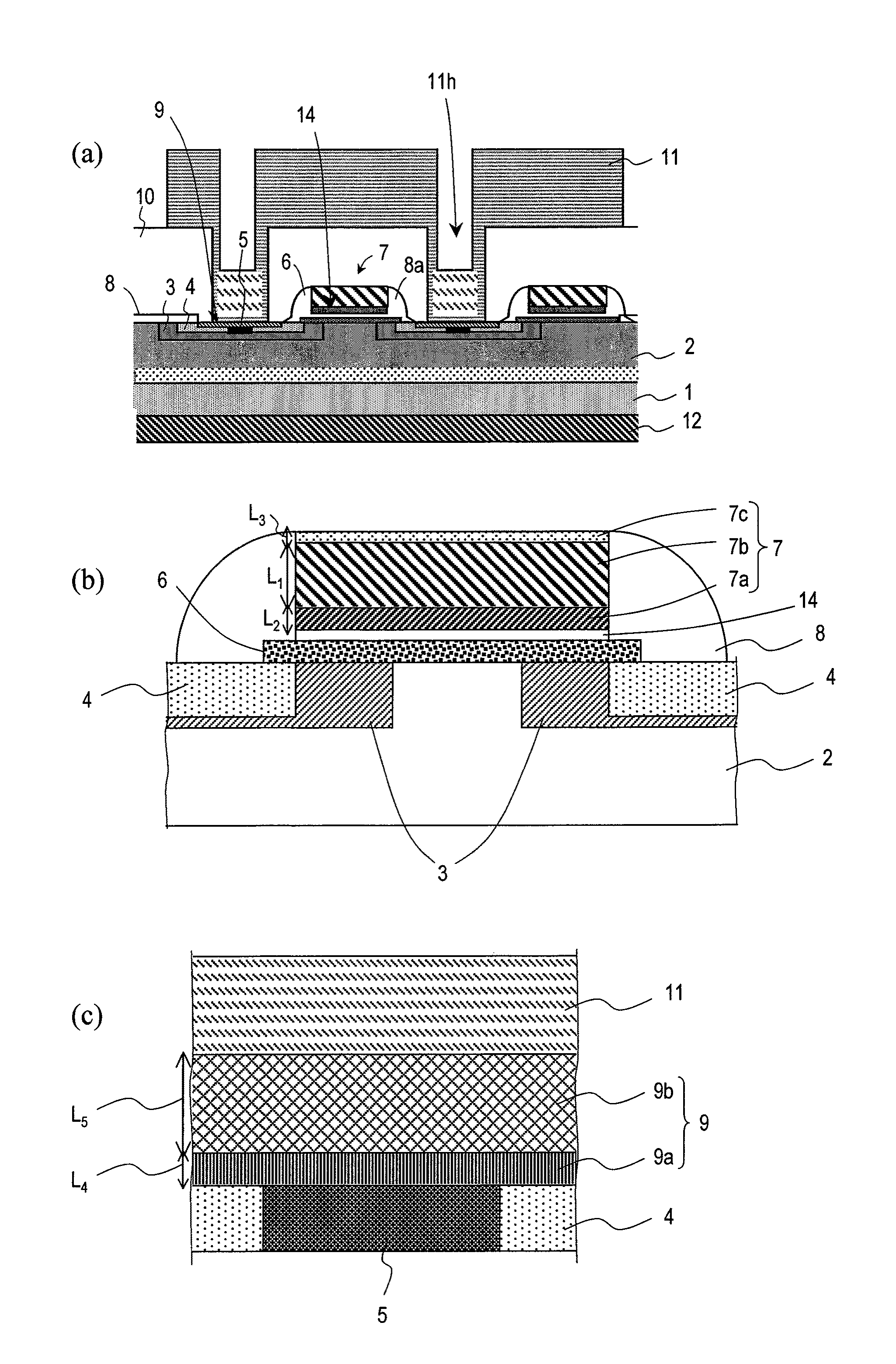
Hereinafter, embodiments of a semiconductor device according to the present invention will be described. The present invention realizes a silicon carbide semiconductor device including an ohmic electrode with no graphite formation and a low-resistance gate electrode, which is preferably usable for an insulating gate-type transistor such as a MISFET, a MOSFET or the like. In the following embodiments, the present invention will be described by way of a vertical type double implantation MISFET as an example.

FIG. 1(a) is a schematic cross-sectional view showing an embodiment of a semiconductor device according to the present invention. A structure of the semiconductor device will be briefly described.

The semiconductor device shown in FIG. 1(a) includes a silicon carbide semiconductor substrate 1 having a silicon carbide layer 2. The silicon carbide semiconductor substrate 1 is an off substrate having an off angle of 8 degrees from the (0001) surface of 4H-SiC. The silicon carbide semic...


PUM

PropertyMeasurementUnit
frequencyaaaaaaaaaa
temperatureaaaaaaaaaa

Abstract

A semiconductor device according to the present invention comprises a silicon carbide semiconductor substrate (1) including a silicon carbide layer (2); a high-concentration impurity region (4) provided in the silicon carbide layer (2); an ohmic electrode (9) electrically connected with the high-concentration impurity region (4); a channel region electrically connected with the high-concentration impurity region; a gate insulating layer (14) provided on the channel region; and a gate electrode (7) provided on the gate insulating layer (14). The ohmic electrode (9) contains an alloy of titanium, silicon and carbon, and the gate electrode (7) contains titanium silicide.

Description

TECHNICAL FIELDThe present invention relates to a semiconductor device including a silicon carbide semiconductor substrate, and in particular to a semiconductor device including a silicon carbide semiconductor substrate having an ohmic electrode and a gate electrode and a method for producing the same.BACKGROUND ARTConventionally, power devices using silicon (Si) semiconductors have been used as devices for power electronics. Devices for power electronics are desired to operate at a higher frequency with a larger current. Various studies for research and development have been made to improve the performance of silicon power devices.However, the performance of the silicon power devices is now approaching the theoretical limit thereof. In addition, power devices are occasionally required to operate in severe environments, for example, at a high temperature or under radiation. Silicon semiconductors are not suitable to use in such severe environments. For these reasons, studies are bei...

Claims


Application Information

Patent Timeline
Patent Type & Authority Patents(United States)
IPC IPC(8): H01L29/78
CPCH01L21/0485H01L21/049H01L29/45H01L29/4975H01L29/66068H01L29/7802H01L29/1608
Inventor HAYASHI, MASASHIHASHIMOTO, SHIN
Owner PANASONIC CORP
Why Eureka
Try Eureka