High fill-factor avalanche photodiode

a photodiode and high filling technology, applied in the field of solid-state photodiodes, can solve the problems of multiplication noise, which is progressively worse, and the signal noise typically associated with linear mode apd operation can be unacceptable for some applications

Active Publication Date: 2012-01-10
MASSACHUSETTS INST OF TECH
View PDF9 Cites 42 Cited by
  • Summary
  • Abstract
  • Description
  • Claims
  • Application Information

AI Technical Summary

Benefits of technology

[0012]The invention provides an avalanche photodiode having a device structure that enables a fill-factor approaching 100% at visible and near-infrared wavelengths, eliminating the need for optical focusing techniques. In the photodiode of the invention, there is provided an n-type active region and a p-type active region. A first one of the n-type and p-type active regions is disposed in a semiconductor substrat...

Problems solved by technology

Although quite adequate for many applications, the signal noise typically associated with linear mode APD operation can be unacceptable for some applications.
The linear mode avalanche gain factor is statistically variable, resulting in so-called multiplication noise, which gets progressively worse as the gain factor is increased by raising the APD reverse bias.
Once the multiplication noise dominates the noise of signal readout circuitry, the APD signal-to-noise ratio is generally unacceptable for many applications.
Specifically, the fraction of the GM-APD structure that is available for ph...

Method used


Image

  • High fill-factor avalanche photodiode
  • High fill-factor avalanche photodiode
  • High fill-factor avalanche photodiode

Examples


example

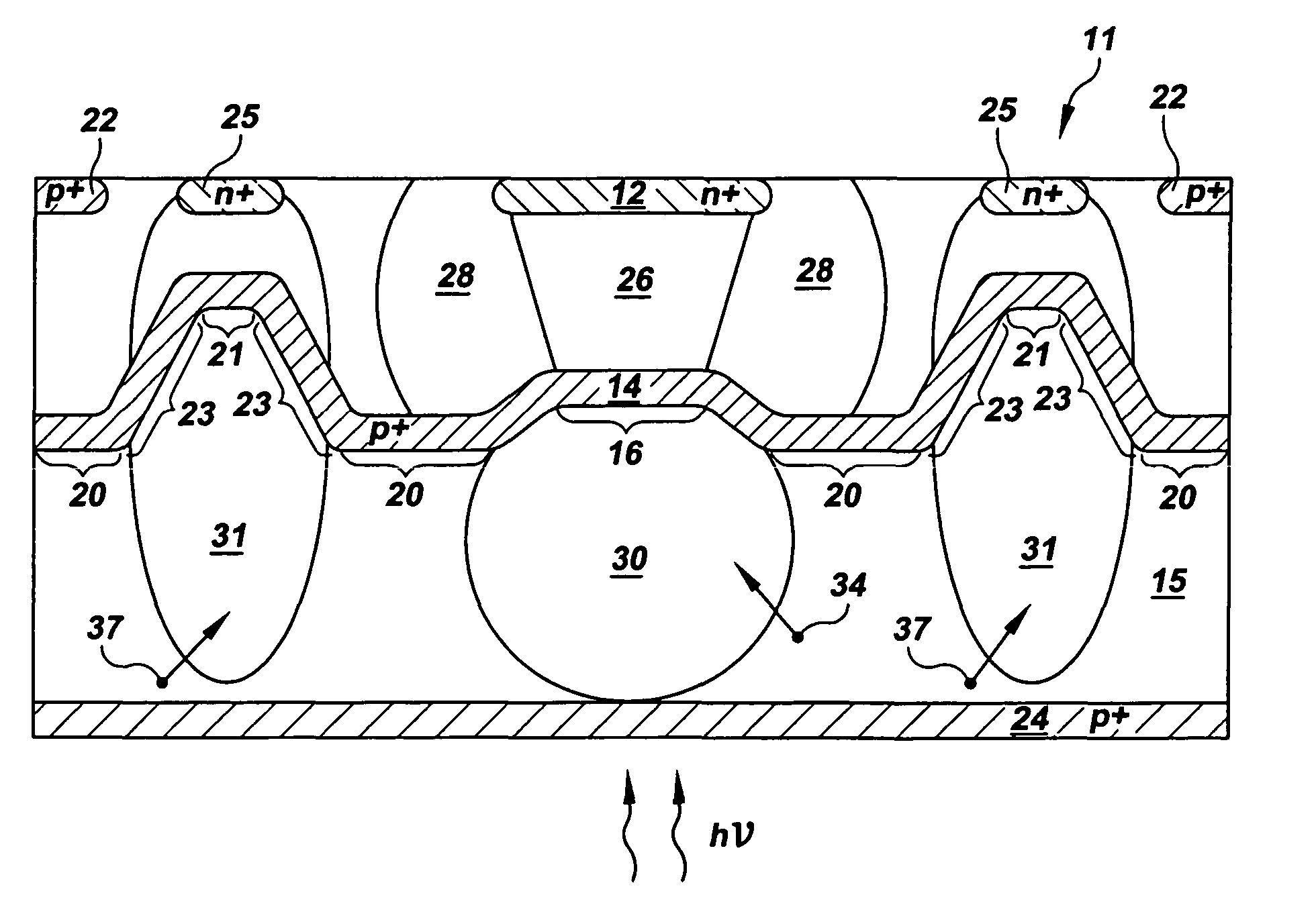
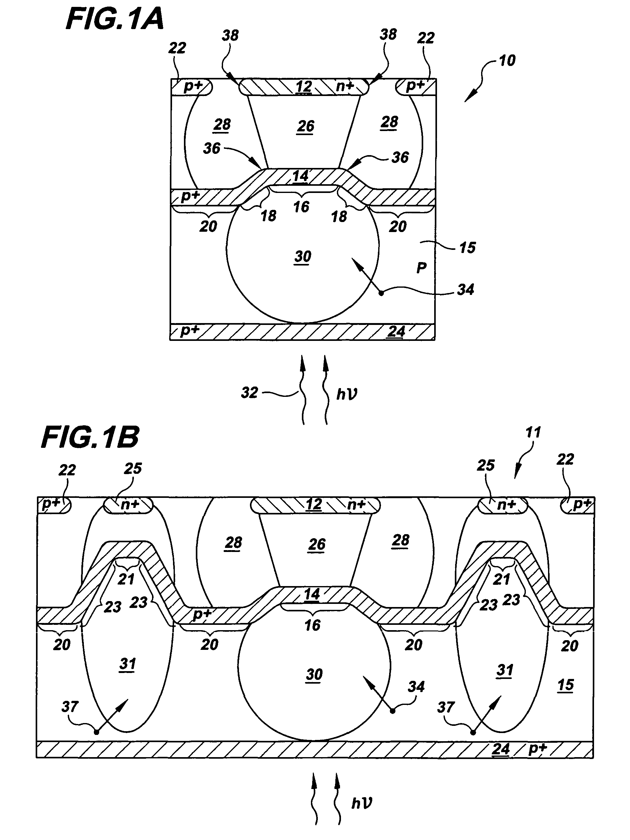
[0073]The avalanche photodiode doping and electric field profile provided by the invention and shown in FIG. 1A were simulated using the Athena and ATLAS simulation tools described above. Reverse bias breakdown and junction punch-through voltages were estimated for the structure to determine an optimum p+ buried layer ion implantation dose and energy given a 5 V cathode voltage range. Based on initial estimates, the depth of the central, elevated high-field zone 16 of the buried layer 14 from the front surface was set at about 0.6 μm. This high-field zone depth corresponds to an APD breakdown voltage of about 30 V with negligible tunneling currents.

[0074]The simulations further specified a buried layer boron ion implantation dose of about 2.8×1012 cm−2 and energy of about 675 KeV, and a tapered oxide region thickness of 500 nm through which the implantation was carried out. These implantation conditions result in good avalanche initiation probability and collection efficiency in the...


PUM


Abstract

A photodiode is provided by the invention, including an n-type active region and a p-type active region. A first one of the n-type and p-type active regions is disposed in a semiconductor substrate at a first substrate surface. A second one of the n-type and p-type active regions includes a high-field zone disposed beneath the first one of the active regions at a first depth in the substrate, a mid-field zone disposed laterally outward of the first active region at a second depth in the substrate greater than the first depth, and a step zone connecting the high-field zone and the mid-field zone in the substrate.

Description

STATEMENT REGARDING FEDERALLY SPONSORED RESEARCH[0001]This invention was made with Government support under Contract No. F19628-00-C-0002 awarded by The Air Force. The Government has certain rights in the invention.BACKGROUND OF INVENTION[0002]This invention relates generally to solid state photodiodes, and in particular relates to avalanche photodiode (APD) device design and fabrication.[0003]Avalanche photodiodes are becoming a popular solid state microfabricated device for illumination detection applications. Avalanche photodiodes that are silicon-based can be microfabricated compatibly with standard CMOS processing. When the p-n junction or p-i-n region of an avalanche photodiode is appropriately reverse-biased, illumination of the APD results in photon absorption that generates electron-hole pairs at a region of high electric field in the vicinity of the reverse bias. This electron-hole pair generation produces an electrical signal corresponding to detection of the illumination...

Claims


Application Information

Patent Timeline
IPC IPC(8): H01L31/107
CPCH01L27/1446H01L31/107
Inventor RENZI, MATTHEW J.AULL, BRIAN F.REICH, ROBERT K.KOSICKI, BERNARD B.
Owner MASSACHUSETTS INST OF TECH
Why Eureka
Try Eureka