Integrated MOSFET and Schottky device
a mosfet and schottky technology, applied in semiconductor devices, diodes, electrical apparatus, etc., can solve the problems that the tmbs type device may not be suitable for a mosfet and schottky device integrated technology, and the tmbs type device may not meet the requirements of the tmbs type device. , to achieve the effect of low leakage, low vf and high leakag
- Summary
- Abstract
- Description
- Claims
- Application Information
AI Technical Summary
Benefits of technology
Problems solved by technology
Method used
Image
Examples
first embodiment
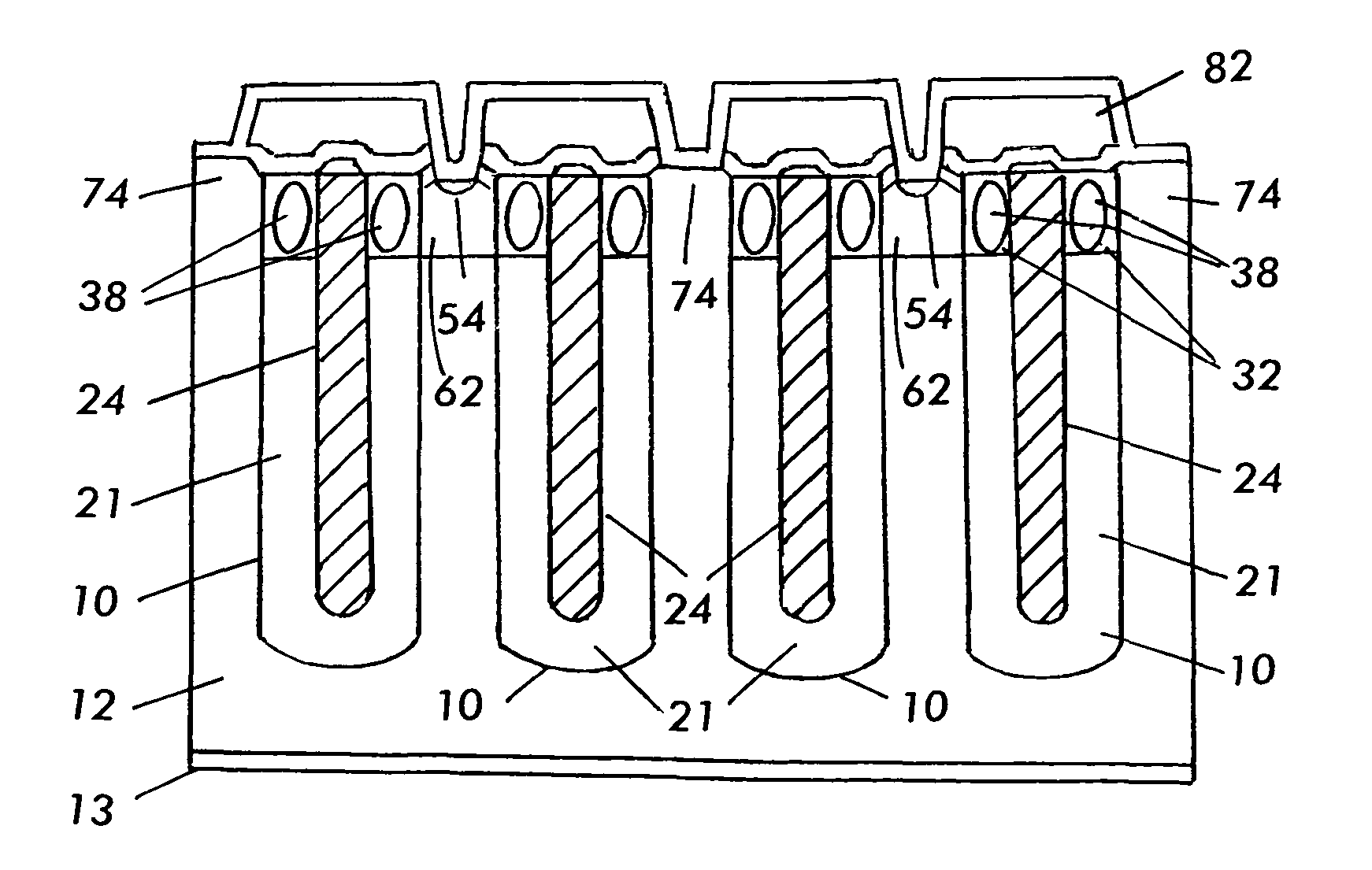
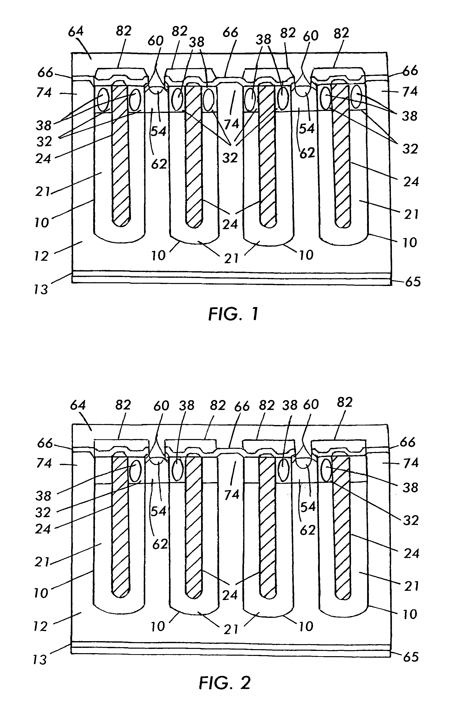
[0011]Referring to FIG. 1, a semiconductor device according to the present invention is preferably a power MOSFET that includes a plurality of spaced deep source trenches 10 formed in a semiconductor body 12, which can be an epitaxially grown silicon body of one conductivity (e.g. N type) disposed over a silicon substrate 13 of the same conductivity. Each trench 10 includes a thick oxide body 21 disposed in the interior and lining at least the bottom and a portion of the sidewalls thereof. A device according to the present invention further includes base regions 62 of the opposite conductivity to body 12 (e.g. P type), source regions 60 of the same conductivity as body 12 formed in base regions 62, a plurality of insulated gate electrodes 38 each insulated from a respective base region 62 by a gate oxide body 32, which is thinner than thick oxide body 21, disposed in trenches 10, a plurality of deep source electrodes 24 which are insulated from, but extend through respective pairs o...
second embodiment
[0016]A device may be useful in cases involving high electric field across the gate oxide.
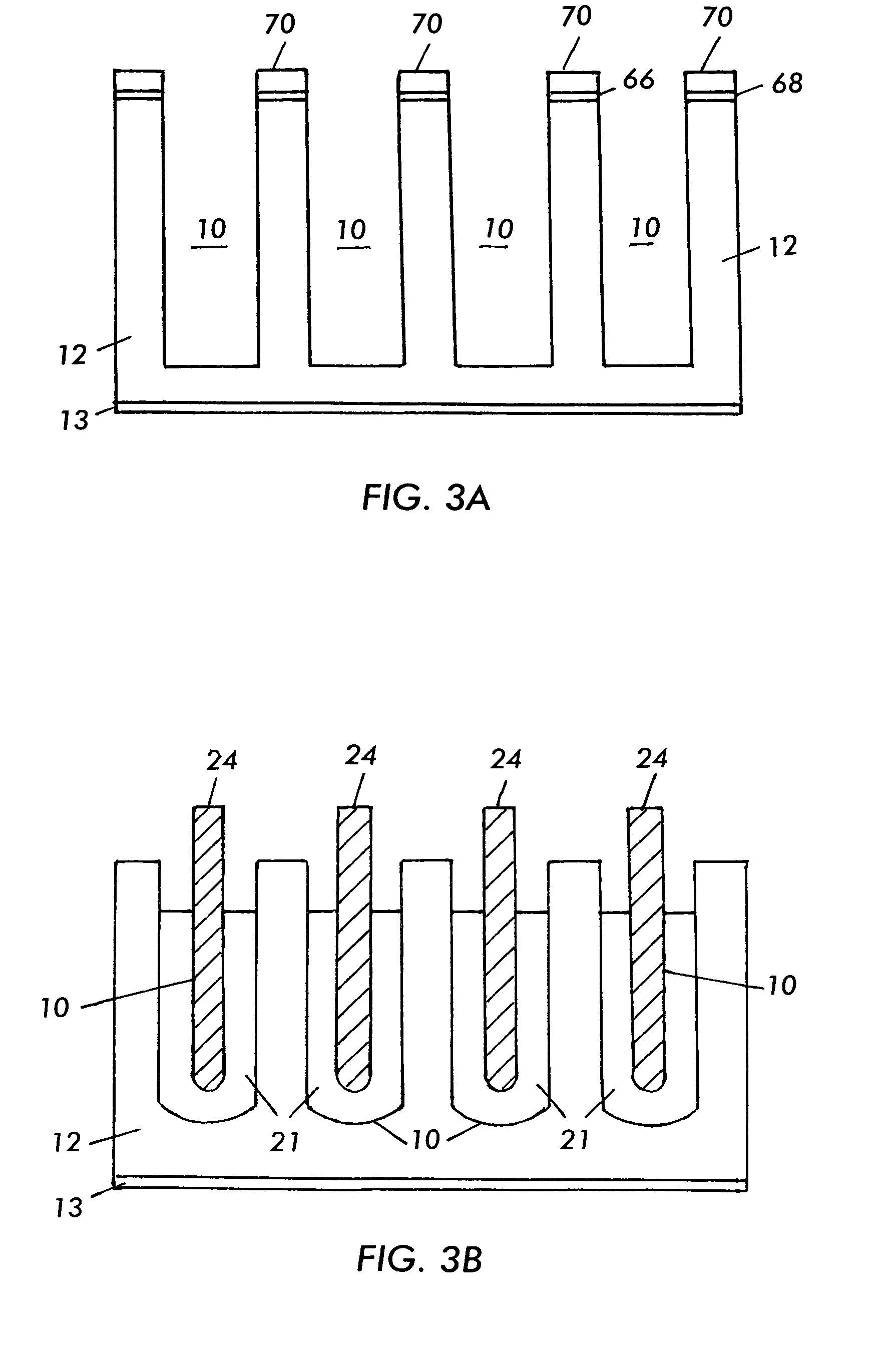
[0017]Referring now to FIG. 3A, to fabricate a device according to the present invention, pad oxide 68 is grown over a surface of semiconductor body 12, a nitride hard mask 70 is deposited over pad oxide 68, and a plurality of source trenches 10 are formed in semiconductor body 12 by etching pad oxide 68 and silicon from the bottom of openings in mask 70.
[0018]Referring next to FIG. 3B, thick oxide 21 is grown inside trenches 10 using any desired method. For example, a method as set forth in U.S. application Ser. No. 11 / 890,849 can be used to form thick oxide 21. The same method can be used to obtain source field electrode 24 as illustrated by FIG. 3B. Namely, field electrodes that extend above the top surface of thick oxide bodies 21.
[0019]Referring next to FIG. 3C, gate oxide 32 is grown on the exposed surfaces of the mesas between trenches 10 in an oxidation process which also oxidizes the ...
PUM
 Abstract
Description
Claims
Application Information


