Manufacturing method of microstructure

a manufacturing method and microstructure technology, applied in the direction of electrical equipment, semiconductor lasers, lasers, etc., can solve the problems of difficult etching of microscopic holes and inability to form holes with high precision, and achieve the effects of increasing the diffraction effect of light, high precision, and microscopic holes

Inactive Publication Date: 2012-03-06
CANON KK
View PDF11 Cites 4 Cited by
  • Summary
  • Abstract
  • Description
  • Claims
  • Application Information

AI Technical Summary

Benefits of technology

[0008]Thus, an object of the present invention is to provide a manufacturing method of a microstructure, which enables production of a microstructure in a GaN semiconductor with high precision.
[0010]According to the present invention, the manufacturing method of a microstructure can be provided, which enables production of a microstructure in a GaN semiconductor with high precision.

Problems solved by technology

However, a GaN semiconductor is a hard material, and therefore, formation of microscopic holes by etching is difficult.
Further, if deep etching is performed, the hole upper portion becomes wider proportionally to the depth, and the hole cannot be formed with high precision.

Method used


Image

  • Manufacturing method of microstructure
  • Manufacturing method of microstructure
  • Manufacturing method of microstructure

Examples


example 1

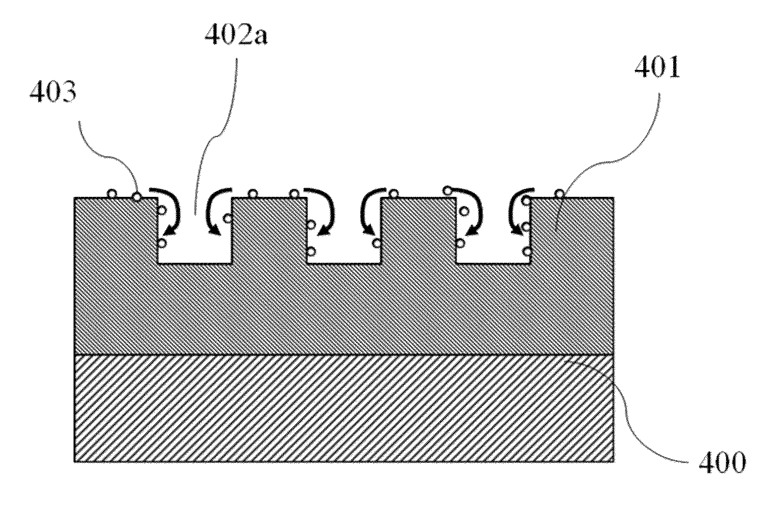
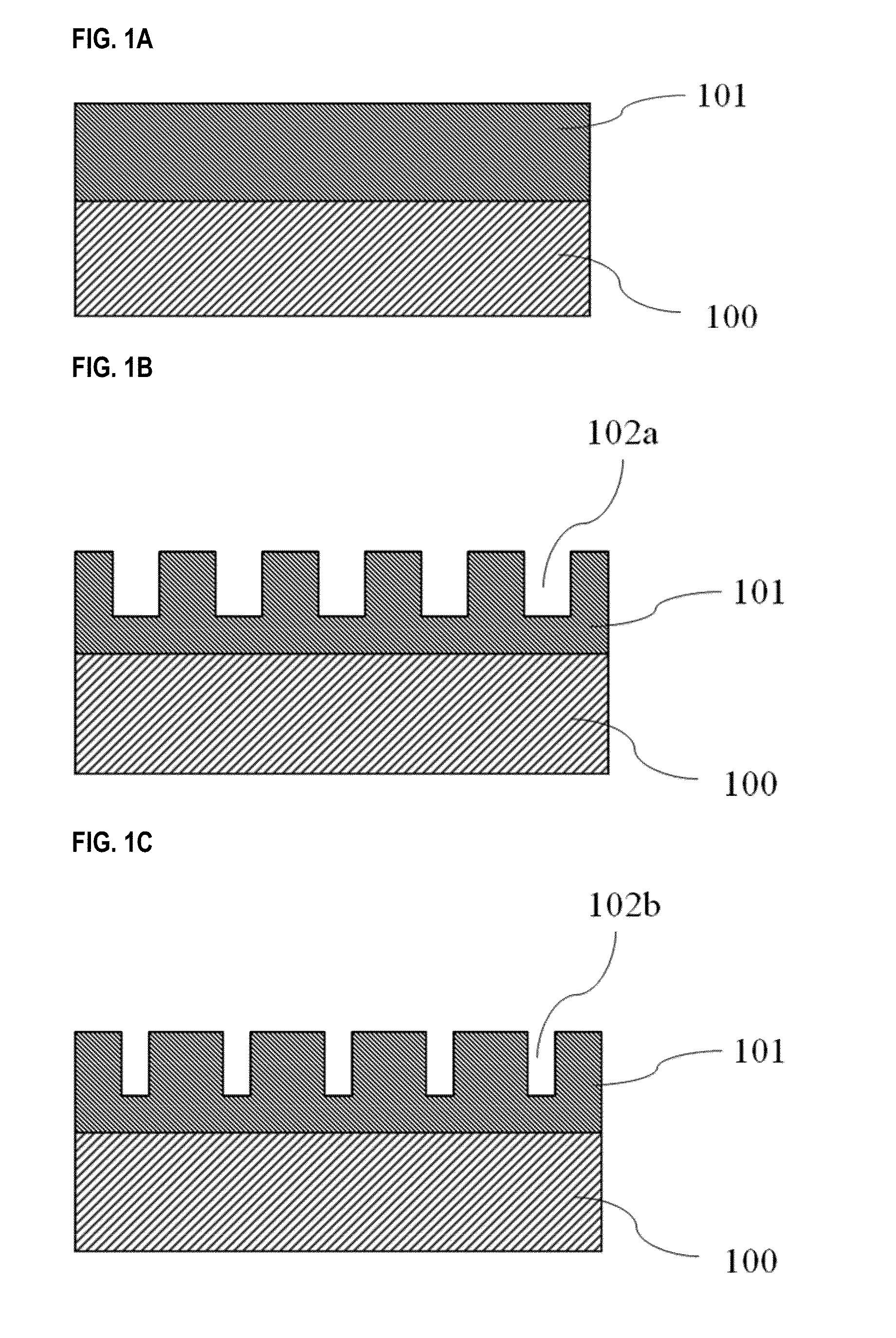
[0064]In the present example, a method for producing a microstructure by using the manufacturing method shown in embodiment 1 will be described. First, as the substrate 100, a sapphire substrate of a c plane is used. Next, the sapphire substrate is set in an MOCVD apparatus. The sapphire substrate is heated to about 1100° C., and the sapphire substrate surface is cleaned in a hydrogen atmosphere. Thereafter, the substrate temperature is lowered to about 500° C., TMG (trimethyl gallium) is supplied at 100 μmol / min, and 5 slm of NH3 is supplied, whereby a low temperature GaN buffer layer of a thickness of 20 nm is formed. Next, the substrate is heated to 1100° C., and GaN is grown by 3 μm as the GaN semiconductor layer 101. Next, the substrate is taken out of the MOCVD apparatus, SiO2 of a thickness of 200 nm is formed on GaN by a sputtering method, and a resist is coated on SiO2. Next, by using electron beam lithography, a circular square-lattice pattern is drawn and developed. The d...

example 2

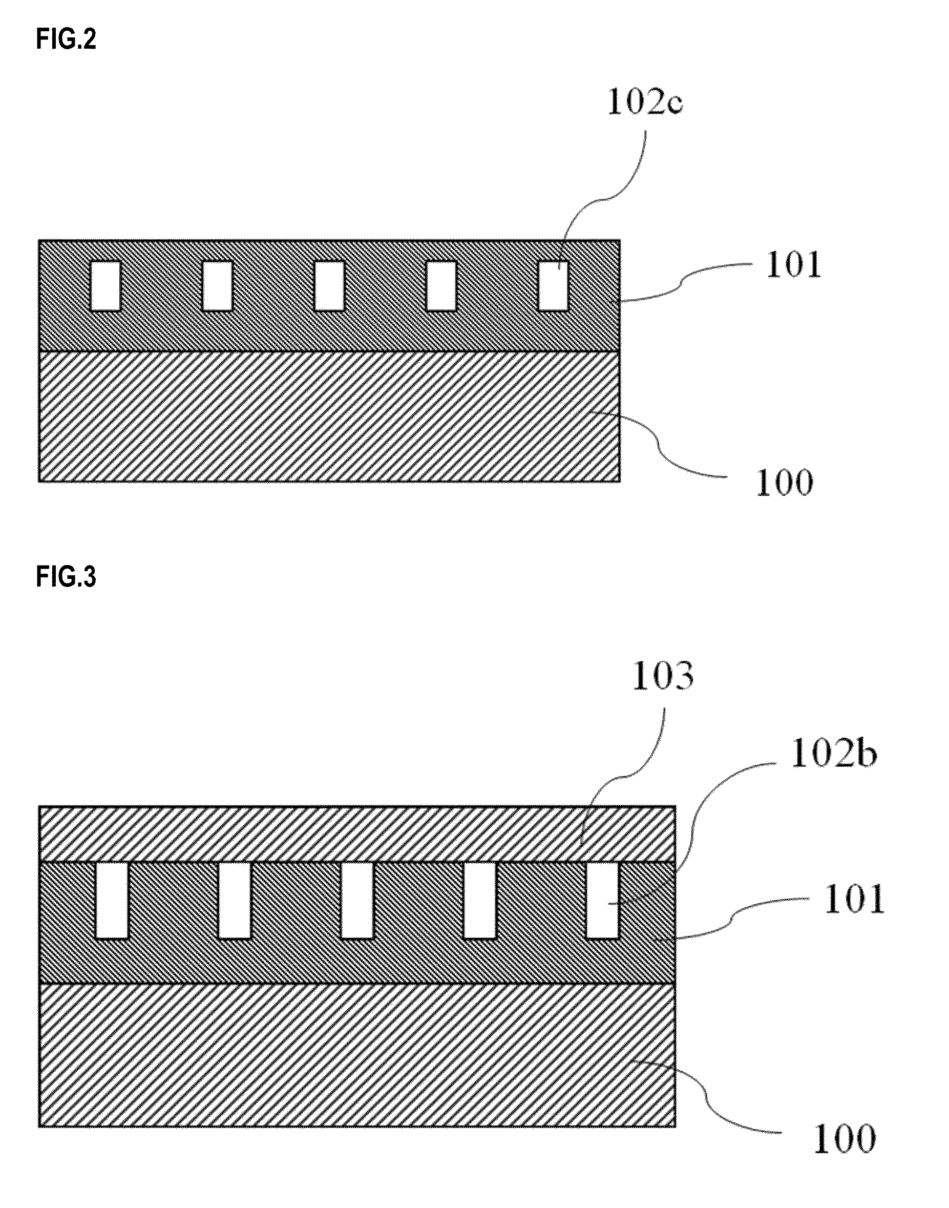
[0067]In the present example, a method for producing a microstructure by using the manufacturing method shown in embodiment 2 will be described. First, as the substrate 100, a GaN substrate of a c plane is used. Next, the GaN substrate is set in the MOCVD apparatus. The GaN substrate is heated to about 1100° C., TMG (trimethyl gallium) is supplied at 100 μmol / min, and 5 slm of NH3 is supplied, whereby GaN is grown by 3 μm as the GaN semiconductor layer 101. Next, the substrate is taken out of the MOCVD apparatus, SiO2 of a thickness of 300 nm is formed on GaN by a plasma CVD apparatus, and a resist is coated on SiO2. Next, by using electron beam lithography, a circular square-lattice pattern is drawn and developed. The diameter of the circle is 150 nm, and the distance between the centers of the adjacent circles is 300 nm.

[0068]Next, with the resist used as a mask, SiO2 is etched by RIE by using CF4 gas.

[0069]A tetragonal lattice pattern is formed on the SiO2, and therefore, this ti...

example 3

[0071]In the present example, a method for producing a microstructure by using the manufacturing method shown in embodiment 3 will be described. First, as the substrate 100, a GaN substrate of a c plane is used. Next, the GaN substrate is set in the MOCVD apparatus. The GaN substrate is heated to about 1100° C., TMGa is supplied at 100 μmol / min, and 5 slm of NH3 is supplied, whereby GaN is grown by 3 μm as the GaN semiconductor layer 101. Next, the substrate is taken out of the MOCVD apparatus, SiO2 of a thickness of 200 nm is formed on the GaN by a plasma CVD apparatus, and a resist is coated on the SiO2. Next, by using electron beam lithography, a circular square-lattice pattern is drawn and developed. The diameter of the circle is 150 nm, and the distance between the centers of the adjacent circles is 300 nm.

[0072]Next, with the resist used as a mask, SiO2 is etched by RIE using CF4 gas. A tetragonal lattice pattern is formed on the SiO2, and therefore, this time, with the SiO2 u...


PUM

PropertyMeasurementUnit
temperatureaaaaaaaaaa

Abstract

A manufacturing method of a microstructure which enables production of a deep and narrow microstructure in a GaN semiconductor with high precision is provided. The manufacturing method of a microstructure for forming a microscopic structure in a semiconductor has a configuration having a first step of forming a first GaN semiconductor layer on a substrate, a second step of forming a first hole by using etching on the first GaN semiconductor layer formed in the first narrow, and a third step of performing heat-treatment at a temperature from 850° C. to 950° C. inclusive under a gas atmosphere including nitrogen, in order to form a second narrow in which a diameter of the first hole h formed in the second step is made narrower than the diameter of the first hole in an in-plane direction of the substrate.

Description

CROSS-REFERENCE TO RELATED APPLICATIONS[0001]This application is a continuation of International Application No. PCT / JP2010 / 004783, filed Jul. 28, 2010, which claims the benefit of Japanese Patent Application No. 2009-178401, filed Jul. 30, 2009.BACKGROUND OF THE INVENTION[0002]1. Field of the Invention[0003]The present invention relates to a manufacturing method of a microstructure, particularly relates to a manufacturing method for forming a microscopic structure inside a semiconductor, and relates to an art for use in a method for manufacturing a light emitting device using a photonic crystal.[0004]2. Description of the Related Art[0005]In recent years, a surface-emitting laser using a two-dimensional photonic crystal has been developed. A photonic crystal has the structure in which a refractive index profile is provided in a wavelength size of light, and a photonic crystal which acts on visible light is in a size of several tens nm to several hundreds nm. Such a two-dimensional ...

Claims


Application Information

Patent Timeline
Patent Type & Authority Patents(United States)
IPC IPC(8): H01L21/00
CPCB82Y20/00H01L21/02389H01L21/0242H01L21/02458H01L21/02513H01L21/0254H01L21/0259H01L21/0262H01L21/02667H01S5/34333H01S5/105H01S5/183H01S2304/04H01S5/11
Inventor KAWASHIMA, TAKESHIHOSHINO, KATSUYUKIKAWASHIMA, SHOICHINAGATOMO, YASUHIRO
Owner CANON KK
Why Eureka
Try Eureka