Method and apparatus for antenna tuning
a technology of antenna impedance matching and antenna, applied in the field of wireless communication, can solve the problems of increasing mismatch between current and voltage, and the phase difference between current and voltage also corresponds to a greater mismatch, so as to reduce the deviation and reduce the mismatch
- Summary
- Abstract
- Description
- Claims
- Application Information
AI Technical Summary
Benefits of technology
Problems solved by technology
Method used
Image
Examples
first embodiment
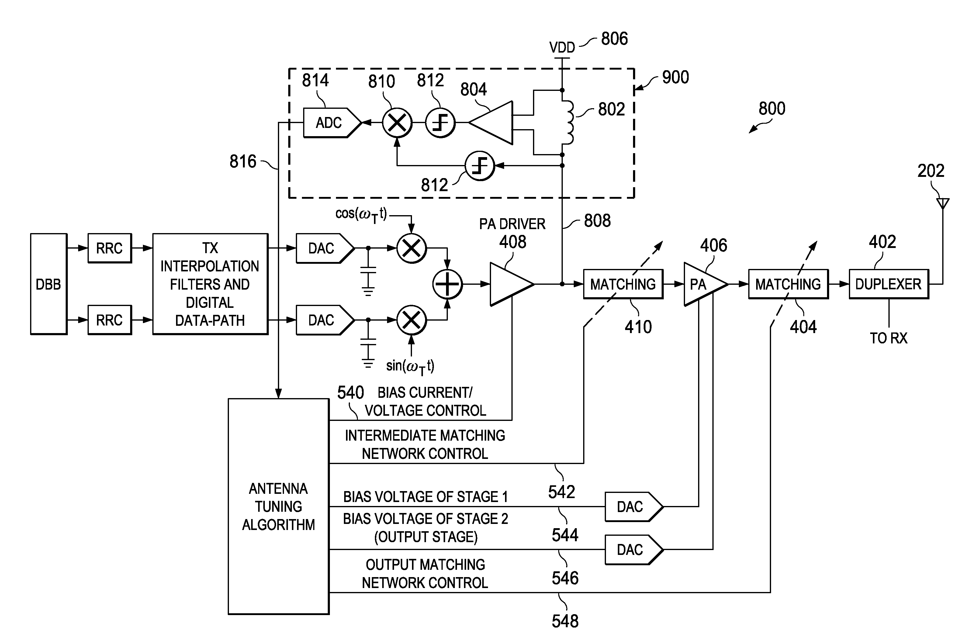
[0041]Referring to FIG. 5, a schematic diagram of an exemplary transmitter 500 with antenna tuning according to the present invention is shown. In this example, RF signals are generated for transmission by low-power RF circuitry in block 520. The illustrated circuit uses digital signal processing (DSP) technology to generate the analog RF signals presented to the input of power amplifier driver 408 in an example wideband code division multiple access (W-CDMA) system, although the present invention may be applied to many different types of wireless signals and systems. Digital baseband processor 522 generates two quadrature modulation outputs that are each filtered by root raised-cosine digital pulse shaping filters 524, further processed by transmit interpolation filters and associated DSP in block 526, followed by conversion from digital to analog by digital-to-analog converters (DACs) 528. The now-analog baseband modulation signals are mixed in mixers 530 with in-phase 532 and qua...
second embodiment
[0048]The reactive part of antenna impedance may change more in response to changes in environment than the resistive (real) part. Thus detecting a change in phase shift between RF voltage and current at the sensed node may provide a more sensitive response to changes in mismatch than sensing the signal amplitude. A second embodiment is next described using a detector circuit capable of generating an error signal based on the relative phase between voltage and current within the transmitter's antenna drive circuit.
[0049]Referring now to FIG. 8, a schematic diagram is shown of a transmitter 800 according to a second embodiment of the present invention. A detector 900 is shown that is capable of generating an error signal based on the relative phase between the RF voltage and current at node 808. To do so, a voltage difference is sensed across choke or inductor 802, where the voltage difference is developed in response to an RF load current flow from supply node 806 at voltage VDD to ...
PUM
 Abstract
Description
Claims
Application Information


