Semiconductor manufacture method

a manufacturing method and semiconductor technology, applied in the direction of individual semiconductor device testing, semiconductor/solid-state device testing/measurement, instruments, etc., can solve problems such as the possibility of erroneous detection, and achieve the effect of preventing local position misalignment, removing abnormal values of position information, and avoiding local position displacemen

Inactive Publication Date: 2012-03-27
FUJITSU SEMICON LTD
View PDF36 Cites 4 Cited by
  • Summary
  • Abstract
  • Description
  • Claims
  • Application Information

AI Technical Summary

Benefits of technology

[0012]An object of the present invention is to improve provision of alignment mark detection in electron beam exposure.
[0014]If noises are superposed upon detectors, amplifiers and the like, there is a possibility of erroneous detection. By utilizing a difference between plural position information, it becomes possible to remove abnormal values of the position information. It is possible to prevent a local position misalignment due to an alignment mark detection error. Local position displacement can be avoided. It is possible to improve an exposure position precision and further improve a pattern position precision.
[0015]A position detection time can be shortened, contributing to reducing the number of manufacturing processes.
[0016]Semiconductor integrated circuit devices can be made fine and highly reliable, and yield and reliability can be improved. By positively using the function of an electron beam exposure method, a micro pattern can be formed at high precision and a position alignment precision can be improved among others. It is possible to contribute to improvement of yield and reliability of semiconductor integrated circuit devices.

Problems solved by technology

If noises are superposed upon detectors, amplifiers and the like, there is a possibility of erroneous detection.

Method used


Image

  • Semiconductor manufacture method
  • Semiconductor manufacture method
  • Semiconductor manufacture method

Examples


first embodiment

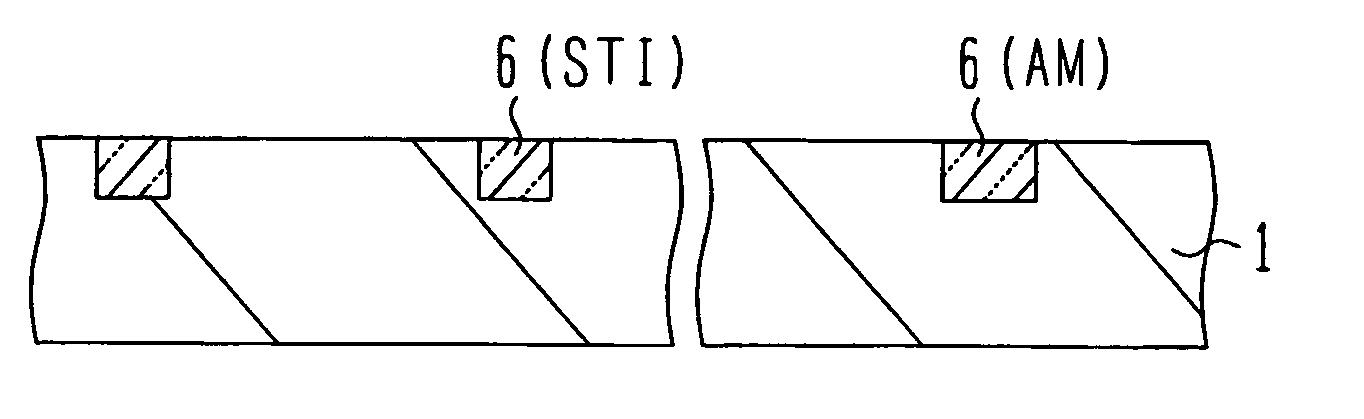
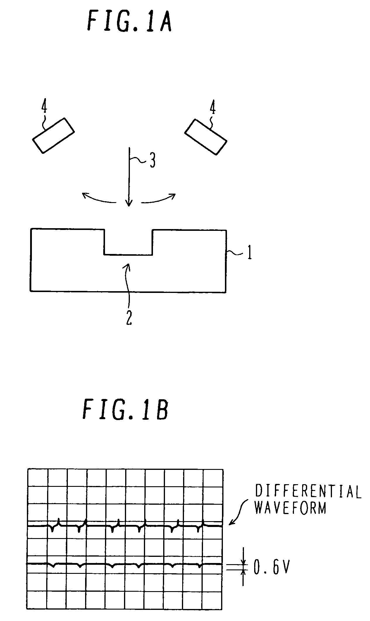
[0050]With reference to FIGS. 4A and 4B, EB exposure of the first embodiment will be described. The process shown in FIG. 3A is executed to form a resist pattern on a silicon substrate, the resist pattern having an opening for an element isolation groove pattern in a semiconductor integrated circuit device area and for an alignment mark pattern. By using the resist pattern as a mask, trenches are etched in the silicon substrate to form steps. Element isolation shallow trenches and alignment marks are formed at the same time. The step is usually about 0.3 μm although it changes depending upon semiconductor integrated circuit devices to be manufactured. An oxide film burying the trench is formed and an unnecessary oxide film is removed by a CMP process to form the structure shown in FIG. 3B. By executing several processes, an insulating film shown in FIG. 3C is formed before contact holes are formed. In order to obtain alignment signals, it is necessary to recover the steps. As descri...

second embodiment

[0062]FIG. 6A shows an example of the layout of alignment marks in a wafer. An alignment mark 9 is disposed near each of four corners of each chip 8 in the wafer.

[0063]FIG. 6B is an enlarged view of one chip area. Alignment marks 9 are disposed without superposing upon scribe lines 10. If inspection after scribing is not necessary, alignment marks may be disposed superposing upon the scribe lines. In FIG. 6A, four alignment marks are disposed near each side of a chip, excepting the outermost side. These marks are assigned to two adjacent chips.

[0064]Alignment mark detection, alignment and exposure are repeated in the group unit including the unit of chip, the unit of chip column and the like. In this case, mark widths W1, W2, W3, W4 of each chip or mark widths W1(i), W2(i), W3(i), W4(i) of each group once obtained are used to determine the reference mark width of, for example, Wref=AVERAGE (W1, W2, W3, W4) or Wref=AVERAGE Σ(W1(i), W2(i), W3(i), W4(i)). The allowable range R of ΔW=|W...

third embodiment

[0067]As shown in FIG. 7, an alignment mark at each position is constituted of a pair of an X-direction mark MX and a Y-direction mark MY. Namely, each alignment mark 9 shown in FIG. 6A is constituted of two marks MX and MY. The widths of the X- and Y-direction marks MX and MY are the same.

[0068]The pair of X- and Y-direction marks are disposed in an area considered having the same process condition, and the X- and Y-direction marks are scanned alternately. An abnormal value is judged from a difference Δ=Wx−Wy between the X-direction mark width Wx and the Y-direction mark width Wy.

[0069]For example, a design value of the mark width is set to 2 μm and an allowable difference is set to 0.10 μm. If the mark width detection results of marks 1, 2, . . . are Wx1=2.10 μm, Wy1=2.11 μm, Wx2=2.40 μm, Wy2=2.10 μm, . . . , an XY difference of the second mark is in excess of the allowable difference. It is judged that there is an erroneous detection, and these values are removed from the positio...


PUM


Abstract

A semiconductor device manufacture method has the steps of: (a) forming a semiconductor device structure in a chip and alignment marks, respectively in a semiconductor wafer; (b) forming a workpiece layer above the semiconductor wafer; (c) exposing the alignment marks; (d) coating an electron beam resist film on the workpiece layer; (e) scanning the alignment marks with an electron beam to obtain plural position information on the alignment marks and obtaining differences between the plural position information; (f) removing abnormal values of position information in accordance with the difference between the plural position information; and (g) performing an electron beam exposure in accordance with plural position information of the alignment marks with the abnormal value being removed. An alignment mark detection precision can be improved in electron beam exposure.

Description

CROSS REFERENCE TO RELATED APPLICATION[0001]This application is based on and claims priority of Japanese Patent Applications No. 2005-100458 filed on Mar. 31, 2005 and No. 2005-279561 filed on Sep. 27, 2005, the entire contents of which are incorporated herein by reference.BACKGROUND OF THE INVENTION[0002]A) Field of the Invention[0003]The present invention relates to a semiconductor device manufacture method, and more particularly to a semiconductor manufacture method by which a workpiece is processed by electron beam exposure.[0004]B) Description of the Related Art[0005]In manufacturing a semiconductor integrated circuit device, lithography is used to form a resist pattern by coating a resist layer on a workpiece layer and exposing and developing it. A precision of lithography is an important factor governing a precision, integration degree and the like of a semiconductor integrated circuit device.[0006]Electron beam (EB) exposure has a high resolution and is suitable for micro pr...

Claims


Application Information

Patent Timeline
Patent Type & Authority Patents(United States)
IPC IPC(8): H01L21/00
CPCB82Y10/00B82Y40/00G03F9/7003H01J37/3045H01J37/3174H01L23/544H01J2237/31793H01L2223/54453H01L2223/5448H01L2924/0002H01L2924/00
Inventor MARUYAMA, TAKASHI
Owner FUJITSU SEMICON LTD
Why Eureka
Try Eureka