Strained CMOS device, circuit and method of fabrication

a technology of cmos and semiconductors, applied in the direction of semiconductor devices, basic electric elements, electrical equipment, etc., can solve the problems of significant process complication, deterioration of pfet device performance, and large challenges, and achieve the effect of improving performan

Active Publication Date: 2012-05-01
GLOBALFOUNDRIES US INC
View PDF17 Cites 78 Cited by
  • Summary
  • Abstract
  • Description
  • Claims
  • Application Information

AI Technical Summary

Benefits of technology

[0010]A semiconductor device and fabrication method include a strained semiconductor layer having a strain in one axis. A long fin and a short fin are formed in the semiconductor layer such that the long fin has a strained length along the one axis. An n-type transistor is formed on the long fin, and a p-type transistor is formed on the short fin. The strain in the n-type transistor improves performance.
[0011]Another method for fabricating a semiconductor device includes providing a providing a Strained Silicon Directly on Insulator (SSDOI) wafer with biaxial tensile strain; patterning long fins and short fins in a semiconductor layer of the wafer such that the long fin has a strained length along its longitudinal axis, and the short fins having dimensions to substantially remove residual strain; forming n-type transistors on the long fins including gate structures and raised active area regions such that the gate structures and the raised active area regions provide anchoring to maintain strain in the strain length of the long fins; and forming p-type transistors on the short fins.
[0012]A semiconductor device includes a strained semiconductor layer fanned into at least one long fin and at least one short fin such that the at least one long fin has a strained length. An n-type transistor is formed on the at least one long fin wherein the strained length improves device operation. A p-type transistor is formed on the short fin.

Problems solved by technology

Furthermore, a dual stress liner (DSL) method, where nitride layers with opposite strains are deposited on n- and p-channel transistors leads to significant process complication and faces great challenges in future technology nodes.
While biaxial tensile strain has a small beneficial effect on NFET performance, it deteriorates PFET device performance.
Such structures impose severe area penalties and manufacturing cost.
The prior art does not provide a manufacturable solution to integrate NFET and PFET devices on a same chip.

Method used


Image

  • Strained CMOS device, circuit and method of fabrication
  • Strained CMOS device, circuit and method of fabrication
  • Strained CMOS device, circuit and method of fabrication

Examples


Embodiment Construction

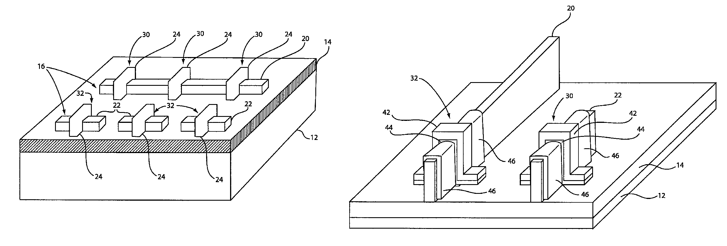
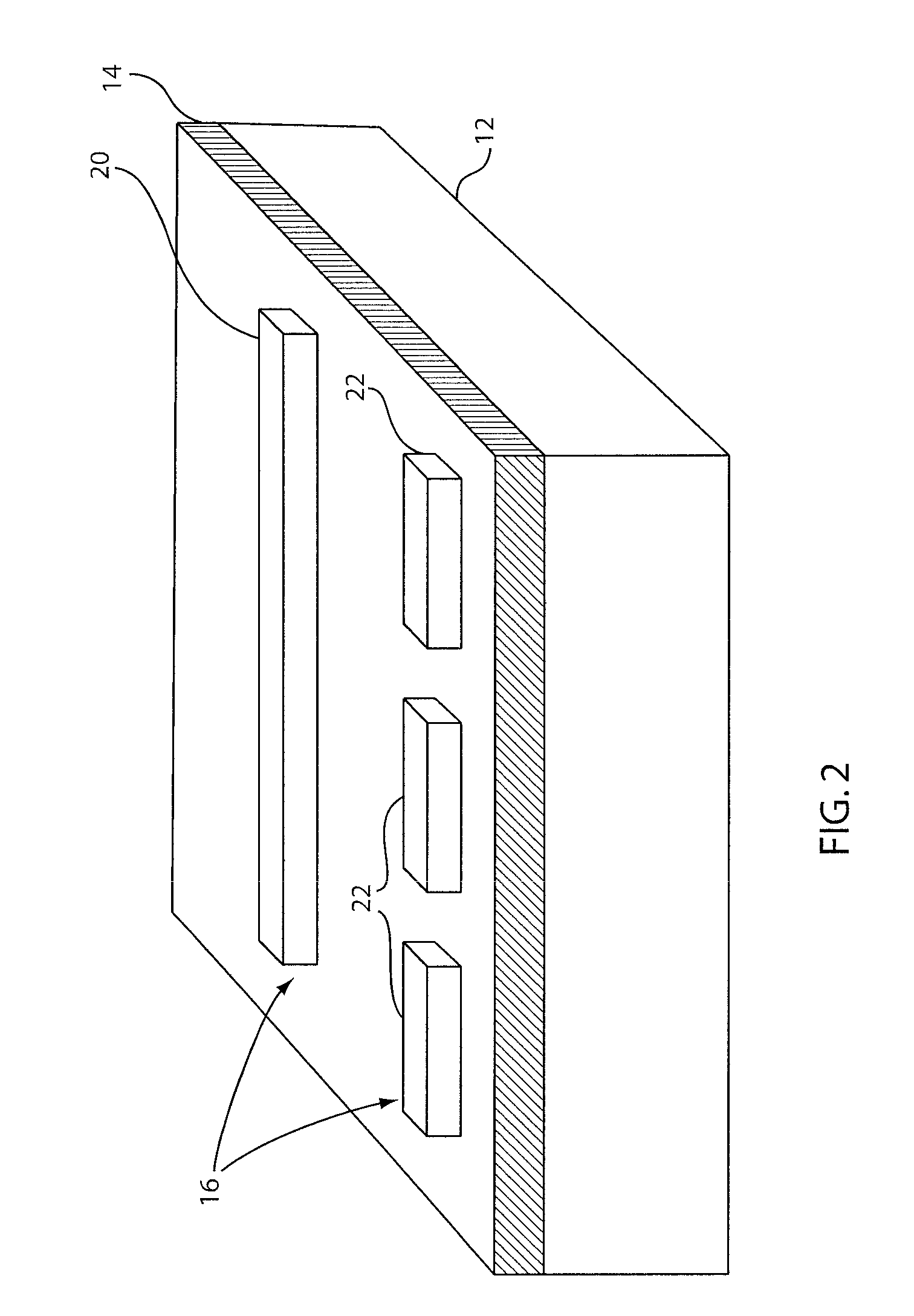
[0023]In accordance with the present principles, a device, circuit and methods for fabricating both n-type field effect transistors (NFETs) and p-type field effect transistors (PFETs) on a same substrate with desired strains for both NFET and PFET devices is provided. In one embodiment, an n-channel metal oxide semiconductor field effect transistor (MOSFET) is fabricated on uniaxially strained Si, wherein the uniaxial tensile strain is achieved by preferential relaxation of global biaxial strain, and a p-channel MOSFET is fabricated on relaxed Si or uniaxially strained Si, wherein uniaxial strain is achieved by local strain engineering, and both device polarities are fabricated on the same substrate. Methods for fabricating these devices are also disclosed.

[0024]One way to achieve enhanced NFET and PFET performance on the same chip is to integrate uniaxially strained SiGe and Si islands on the same substrate, which uses preferential epitaxial growth or layer removal and / or additiona...


PUM


Abstract

A semiconductor device and fabrication method include a strained semiconductor layer having a strain in one axis. A long fin and a short fin are formed in the semiconductor layer such that the long fin has a strained length along the one axis. An n-type transistor is formed on the long fin, and a p-type transistor is formed on the at least one short fin. The strain in the n-type transistor improves performance.

Description

BACKGROUND[0001]1. Technical Field[0002]The present invention relates to semiconductor devices and processes, and more particularly to strained semiconductor materials suitable for different polarity devices on a same substrate.[0003]2. Description of the Related Art[0004]Strained silicon is being used by the semiconductor industry to improve transistor performance. Increased strain levels are desired in future technology nodes (e.g., 32 nm and beyond) to continue to improve transistor performance. In general, there are two methods to apply strain on devices: global and local strain engineering. Global biaxial tensile strain can be readily achieved by growing Si on relaxed SiGe buffer layers, which are grown epitaxially on a Si wafer. However, biaxial tensile strain offers a small enhancement in transistor performance (See, e.g., K. Rim. et al., “Characteristics and device design of sub-100 nm strained Si N- and PMOSFETs,” Symp. VLSI Technol., pp. 98-99, 2002.).[0005]Local strain en...

Claims


Application Information

Patent Timeline
Patent Type & Authority Patents(United States)
IPC IPC(8): H01L27/12
CPCH01L21/845H01L27/1211H01L29/7849
Inventor BEDELL, STEPHEN W.CHENG, KANGGUODORIS, BRUCE B.KHAKIFIROOZ, ALISADANA, DEVENDRA K.SHAHIDI, GHAVAM G.
Owner GLOBALFOUNDRIES US INC
Why Eureka
Try Eureka