Reliable charge pump circuit

a charge pump and circuit technology, applied in the field of electronic devices, can solve the problems of whole feedback loop oscillation, charge pump cannot work properly, and the tracking and locking frequency of input signals will fail, so as to prevent deadlock or oscillation

Inactive Publication Date: 2012-05-15
IPGOAL MICROELECTRONICS (SICHUAN) CO LTD
View PDF20 Cites 3 Cited by
  • Summary
  • Abstract
  • Description
  • Claims
  • Application Information

AI Technical Summary

Benefits of technology

[0019]An objective of the present invention is to provide a reliable charge pump circuit which can prevent deadlock or oscillation during the frequency locking process, so as to ensure proper functionality.
[0027]wherein the anti-lock circuit comprises a current source and a diode-connected (the “diode-connected” is one type of transistor connections in a complementary metal oxide semiconductor (CMOS) integrated circuit, which is characterized as its drain node and its gate node are connected) NMOS transistor, which is equivalent of adding a low resistor to an output node of the operational amplifier, so as to increase the driving strength of the operational amplifier to two NMOS transistors, hence, to prevent deadlock.
[0028]The anti-lock circuit further comprises a MOS capacitor connected to a noninverting input node of the operational amplifier, for improving stability.
[0029]The diode-connected NMOS transistor is in saturation region and conducting all the time, so driven by the current source and the diode-connected NMOS transistor, the voltage value of the output node of the operational amplifier is always higher than either threshold voltage value of two NMOS transistors which are connected to the output node of the operational amplifier, then the two NMOS transistors will not be cut-off, so as to solve the deadlock problem.
[0042]Given two poles W1=1 / (R1′×C1), W2=1 / (R2×C2′), (the pole is a concept in signals and systems, which means that a transfer function reaches infinity.) when W1 gets larger, W2 gets smaller, and therefore, the two poles W1, W2 are separated. W2 becomes main pole, W1 becomes secondary pole, W1 is far away from the main pole W2, so that the phase margin is increased, and stability is improved. Therefore, the key point of improving stability is to separate the pole W1 from W2 in the conventional charge pump circuit.
[0043]The beneficial effects of the present invention are illustrated as follows: firstly, the reliable charge pump circuit can improve stability of the charge pump circuit, so as to make the charge pump circuit more stable and reliable. Secondly, the reliable charge pump circuit can prevent deadlock caused by multiple stable status, so as to improve production yield.

Problems solved by technology

During this process, if the output voltage of the charge pump is locked on a certain value owing to some reasons such as circuit's positive feedback, or existence of multiple stable status, the process for tracking and locking the frequency of the input signal will fail.
On the other hand, if the phase margin of the feedback loop is not enough, that is, the phase of the loop gain is larger than 135 degree when the magnitude of the loop gain is unity, then the whole feedback loop will oscillate, and the charge pump could not work properly.
Making a small signal analysis for entire circuit system, once the phase margin of the negative feedback loop is not enough, the system will oscillate, and the charge pump will not work properly.
However, once there are some disturbances making the net OUT higher than the voltage of the net14 during working process, the problem described above will still occur.
here, W1=1 / (R1·C1), W2=1 / (R2·C2), because the two poles are approximately equal to each other, resulting that the phase margin is not enough, so the entire system is not stable.

Method used


Image

  • Reliable charge pump circuit
  • Reliable charge pump circuit
  • Reliable charge pump circuit

Examples


Embodiment Construction

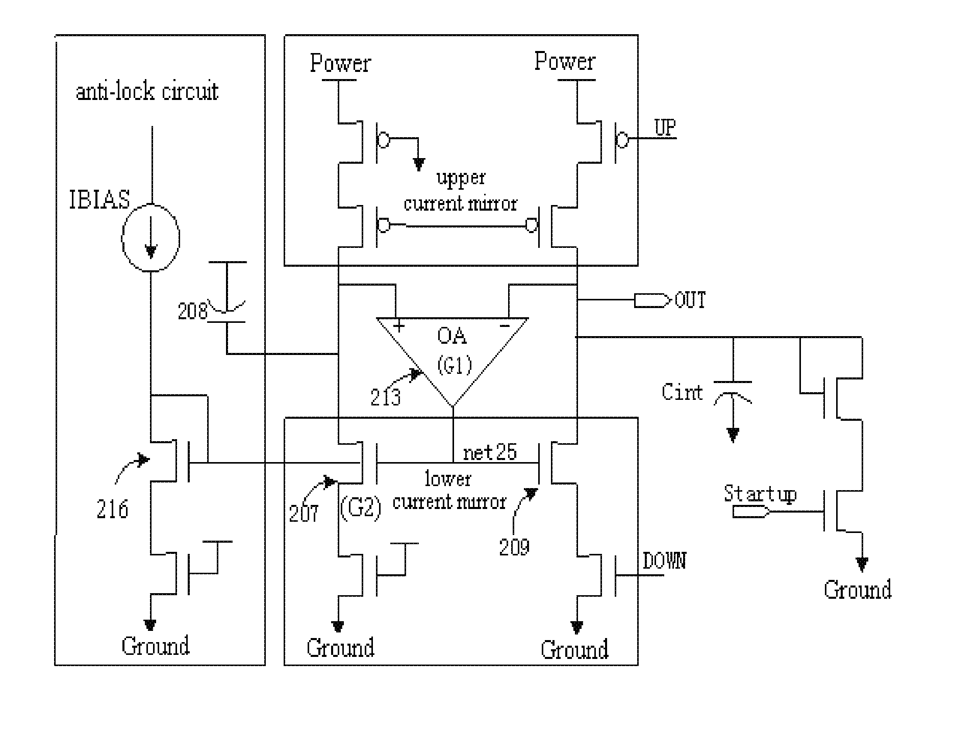
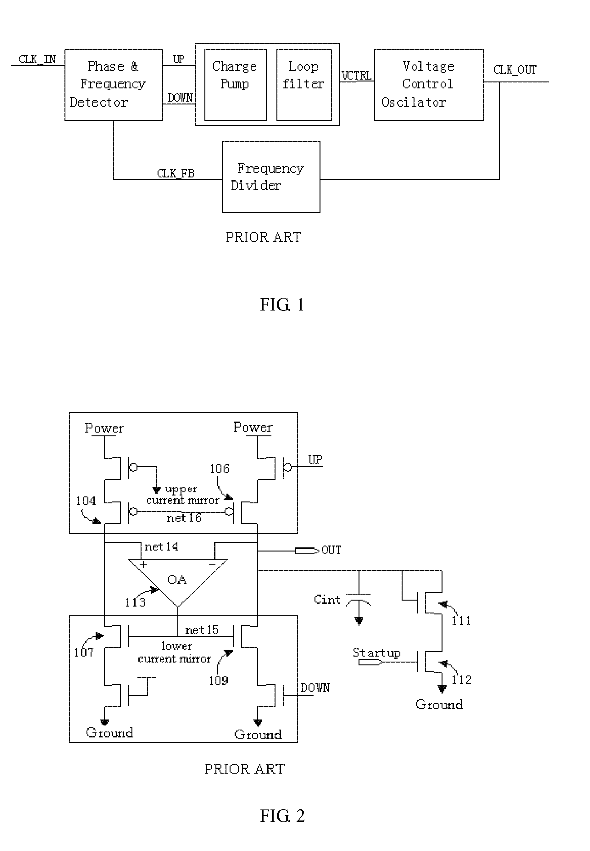
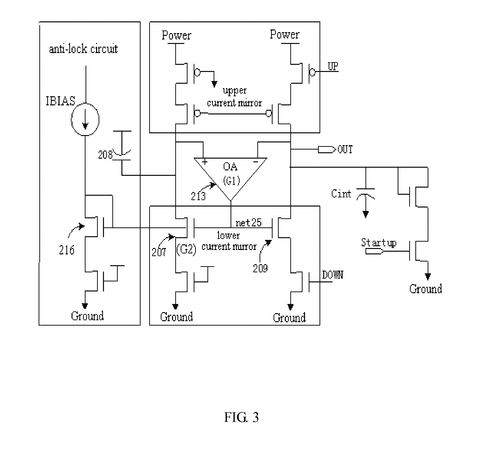
[0052]As shown in FIG. 3, a reliable charge pump circuit, comprises an operational amplifier (OA) 213; an upper current mirror; a lower current mirror; an integral capacitor Cint; a startup circuit; and an anti-lock circuit. The anti-lock circuit comprises a current source IBIAS and a diode-connected (the “diode-connected” is one type of transistor connections in a complementary metal oxide semiconductor (CMOS) integrated circuit, which is characterized as its drain node and its gate node are connected) NMOS transistor 216, which is equivalent of adding a low resistor to an output of the operational amplifier, so as to increase the driving strength of the operational amplifier to two NMOS transistors 207, 209 which are connected to an output node of the operational amplifier, hence to prevent deadlock.

[0053]The anti-lock circuit further comprises a MOS capacitor 208 connected to a noninverting input node of the operational amplifier, for improving stability.

[0054]The diode-connected...


PUM


Abstract

A reliable charge pump circuit includes an operational amplifier; an upper current mirror; a lower current mirror; a startup circuit; and an anti-lock circuit, wherein the anti-lock circuit includes a current source and a diode-connected NMOS transistor, which increases the driving strength of the operational amplifier to two NMOS transistors connected to an output node of the operational amplifier, so as to prevent deadlock caused by multiple stable status and improve production yield.

Description

BACKGROUND OF THE PRESENT INVENTION[0001]1. Field of Invention[0002]The present invention relates to electronic field, and more particularly, relates to a reliable charge pump circuit which can ensure proper functionality in all conditions.[0003]2. Description of Related Arts[0004]Both Phase-Locked Loop (PLL) and Delay Locked Loop (DLL), require to obtain a phase difference between their own output signal and input reference signal, then integrate this phase difference via a charge pump circuit, and the integrated result is reflected in control voltage VCTRL in form of varying quantity of voltage. The control voltage VCTRL is used to control a voltage controlled oscillator VCO or a voltage controlled delay line VCDL, until their phases are synchronous. The system to achieve above phase-locked loop lock process (PLL) is shown in FIG. 1.[0005]The relevant reference is the following U.S. patents:[0006]CHARGE PUMP CIRCUIT[0007]U.S. Pat. No. 6,535,051 B2 March 2003 Kyu-hyoun Kim[0008]HIG...

Claims


Application Information

Patent Timeline
Patent Type & Authority Patents(United States)
IPC IPC(8): H03L7/06
CPCH03L7/0895
Inventor TANG, WEIYUN
Owner IPGOAL MICROELECTRONICS (SICHUAN) CO LTD
Why Eureka
Try Eureka