High speed light emitting semiconductor methods and devices

a semiconductor and high-speed technology, applied in the direction of semiconductor lasers, lasers, electric lighting sources, etc., can solve the problem of parasitic capacitance limitations in the microwave performance of an hblet, and achieve the effects of reducing lateral extrinsic “parasite-like” rc charging, fast recombination dynamics of intrinsic transistors, and improving both electrical and optical characteristics

Active Publication Date: 2012-05-15
QUANTUM ELECTO OPTO SYST +1
View PDF26 Cites 21 Cited by
  • Summary
  • Abstract
  • Description
  • Claims
  • Application Information

AI Technical Summary

Benefits of technology

[0009]Applicant has discovered that the lateral scaling of a heterojunction bipolar light-emitting transistor (LET) or a tilted charge light-emitting diode can improve both electrical and optical characteristics. For example, the fast recombination dynamics of the intrinsic transistor can be harnessed by scaling down an emitter aperture to reduce lateral extrinsic “parasitic-like” RC charging. The fast spontaneous modulation speeds, together with the high yield and reliability due to ease of fabrication and threshold-less operation of the LET or tilted charge light-emitting diode, offer attractive alternatives to laser sources, especially for use in short range optical data communications and interconnections.
[0012]In accordance with an embodiment of a further form of the invention, a method is set forth for producing a high frequency optical signal component representative of a high frequency electrical signal component, including the following steps: providing a layered semiconductor structure including a semiconductor drain region comprising at least one drain layer, a semiconductor base region disposed on said drain region and including at least one base layer, and a semiconductor emitter region disposed on a portion of said base region and comprising an emitter mesa that includes at least one emitter layer; providing, in said base region, at least one region exhibiting quantum size effects; providing a base / drain electrode having a first portion on an exposed surface of said base region and a further portion coupled with said drain region, and providing an emitter electrode on the surface of said emitter region; applying signals with respect to said base / drain and emitter electrodes to produce light emission from said base region; providing an optical window or cavity for said light emission in the region between said first portion of the base / drain electrode and said emitter electrode; and scaling the lateral dimensions of said optical window or cavity to control the speed of light emission response to said high frequency electrical signal component.

Problems solved by technology

91, 033505, 2007; G. Walter, C. H. Wu, H. W. Then, M. Feng, and N. Holonyak, Jr., “4.3 GHz optical bandwidth light emitting transistor,” (submitted to Appl. Phys. Lett.), 2009, supra) In practice, despite the high intrinsic speed of the HBT, the microwave performance of an HBLET is limited by parasitic capacitances, due to factors including extrinsic carrier transport effects and to the need to include light extraction features (such as oxide apertures) not present in traditional high speed HBT devices.

Method used


Image

  • High speed light emitting semiconductor methods and devices
  • High speed light emitting semiconductor methods and devices
  • High speed light emitting semiconductor methods and devices

Examples


Embodiment Construction

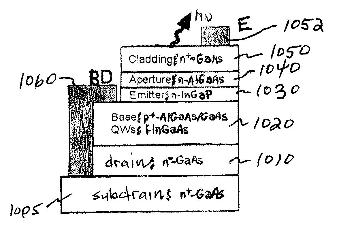
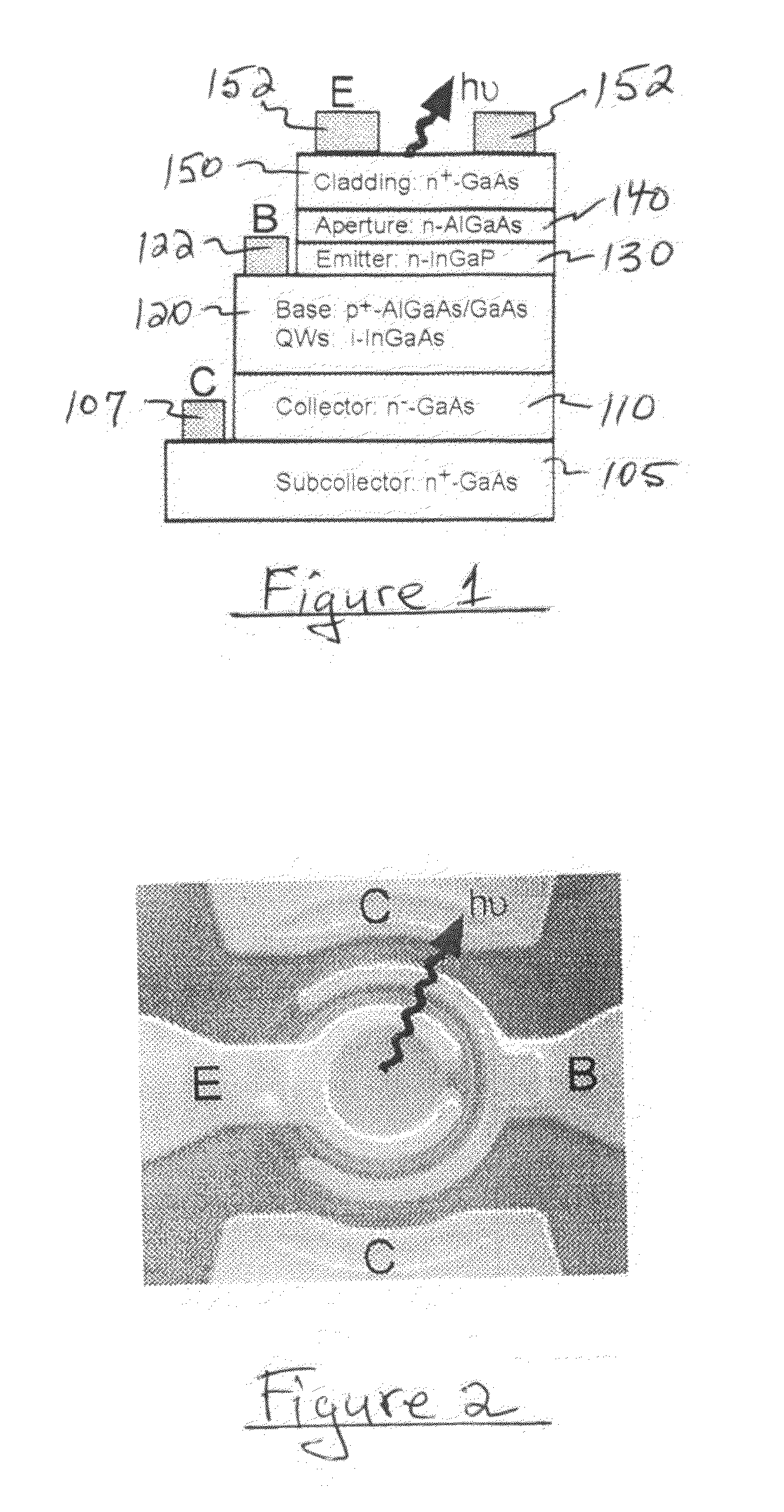
[0026]For an example of an embodiment of the invention, the epitaxial layers of the crystals used for a heterojunction bipolar light emitting transistor (HBLET), fabricated using MOCVD, included a 3000 Å n-type heavily doped GaAs buffer layer, followed by a 500 Å n-type Al0.30Ga0.60As layer, a graded Al0.30Ga0.70As to Al0.90Ga0.10As oxide buffer layer, a 600 Å n-type Al0.98Ga0.02As oxidizable layer, and then a graded Al0.90Ga0.10As to Al0.30Ga0.70As oxide buffer layer that completes the bottom cladding layers. These layers are followed by a 557 Å n-type subcollector layer, a 120 Å In0.49Ga0.51P etch stop layer, a 2871 Å undoped GaAs collector layer, and a 1358 Å average p-doped 3×1019 cm−3 AlGaAs / GaAs graded base layer (the active layer), which includes two undoped 112 Å InGaAs quantum wells (designed for λ≈980 nm). The epitaxial HBTL structure is completed with the growth of the upper cladding layers, which include a 511 Å n-type In0.49Ga0.51P wide-gap emitter layer, a graded Al0.3...


PUM


Abstract

A method for producing a high frequency optical signal component representative of a high frequency electrical input signal component, includes the following steps: providing a semiconductor transistor structure that includes a base region of a first semiconductor type between semiconductor emitter and collector regions of a second semiconductor type; providing, in the base region, at least one region exhibiting quantum size effects; providing emitter, base, and collector electrodes respectively coupled with the emitter, base, and collector regions; applying electrical signals, including the high frequency electrical signal component, with respect to the emitter, base, and collector electrodes to produce output spontaneous light emission from the base region, aided by the quantum size region, the output spontaneous light emission including the high frequency optical signal component representative of the high frequency electrical signal component; providing an optical cavity for the light emission in the region between the base and emitter electrodes; and scaling the lateral dimensions of the optical cavity to control the speed of light emission response to the high frequency electrical signal component.

Description

PRIORITY CLAIMS[0001]This is a continuation-in-part of U.S. patent application Ser. No. 12 / 655,806, filed Jan. 7, 2010, incorporated herein by reference, which, in turn, claimed priority from three U.S. Provisional Patent Applications; namely, U.S. Provisional Application Ser. No. 61 / 204,560, filed Jan. 8, 2009, U.S. Provisional Application Ser. No. 61 / 204,602, filed Jan. 8, 2009, and U.S. Provisional Application Ser. No. 61 / 208,422, filed Feb. 24, 2009. Priority is also claimed from U.S. Provisional Patent Application Ser. No. 61 / 212,951, filed Apr. 17, 2009, and from U.S. Provisional Patent Application Ser. No. 61 / 268,119, filed Jun. 9, 2009, and both of said last mentioned U.S. Provisional Patent Applications are incorporated herein by reference.GOVERNMENT RIGHTS[0002]This invention was made with Government support, and the Government has certain rights in the invention.RELATED APPLICATION[0003]The subject matter of this Application relates to subject matter disclosed in copendin...

Claims


Application Information

Patent Timeline
Patent Type & Authority Patents(United States)
IPC IPC(8): H01S3/00
CPCB82Y20/00H01L33/0016H01L33/30H01S5/06203H01S5/34313H01L33/38H01S5/06213H01S5/183H01S5/1835
Inventor WALTER, GABRIELFENG, MILTONHOLONYAK, JR., NICKTHEN, HAN WUIWU, CHAO-HSIN
Owner QUANTUM ELECTO OPTO SYST
Why Eureka
Try Eureka