

Graphene growth on a carbon-containing semiconductor layer
a technology of graphene and silicon carbide, which is applied in the direction of instruments, record information storage, transportation and packaging, etc., can solve the problems of prior attempts to grow a single crystalline silicon carbide layer on a single crystalline silicon substrate, polycrystalline silicon carbide growth on silicon, and inability to provide a 200 mm or 300 mm substrate containing a graphene layer
- Summary
- Abstract
- Description
- Claims
- Application Information
AI Technical Summary
Benefits of technology
Problems solved by technology
Method used
Image

Examples
first embodiment
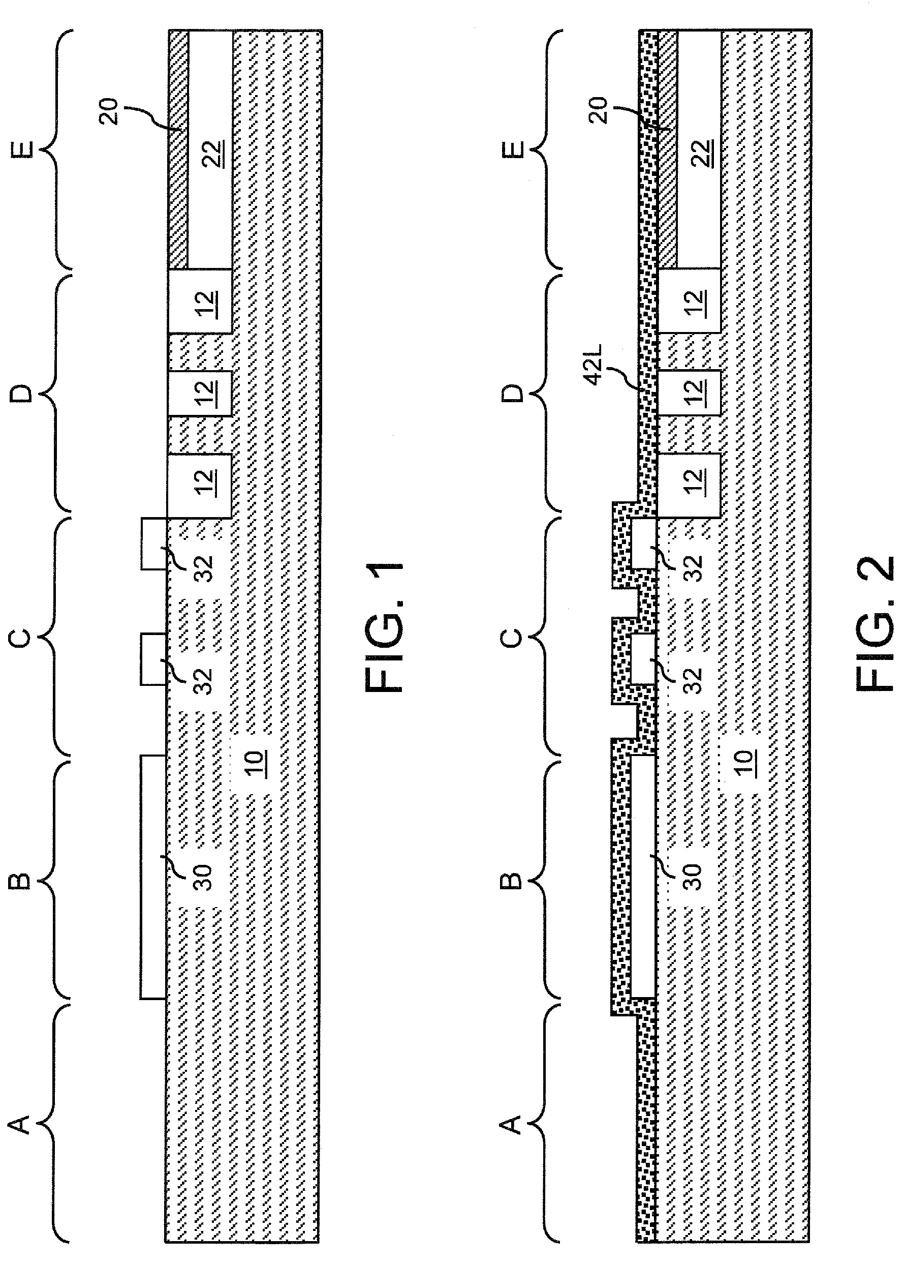
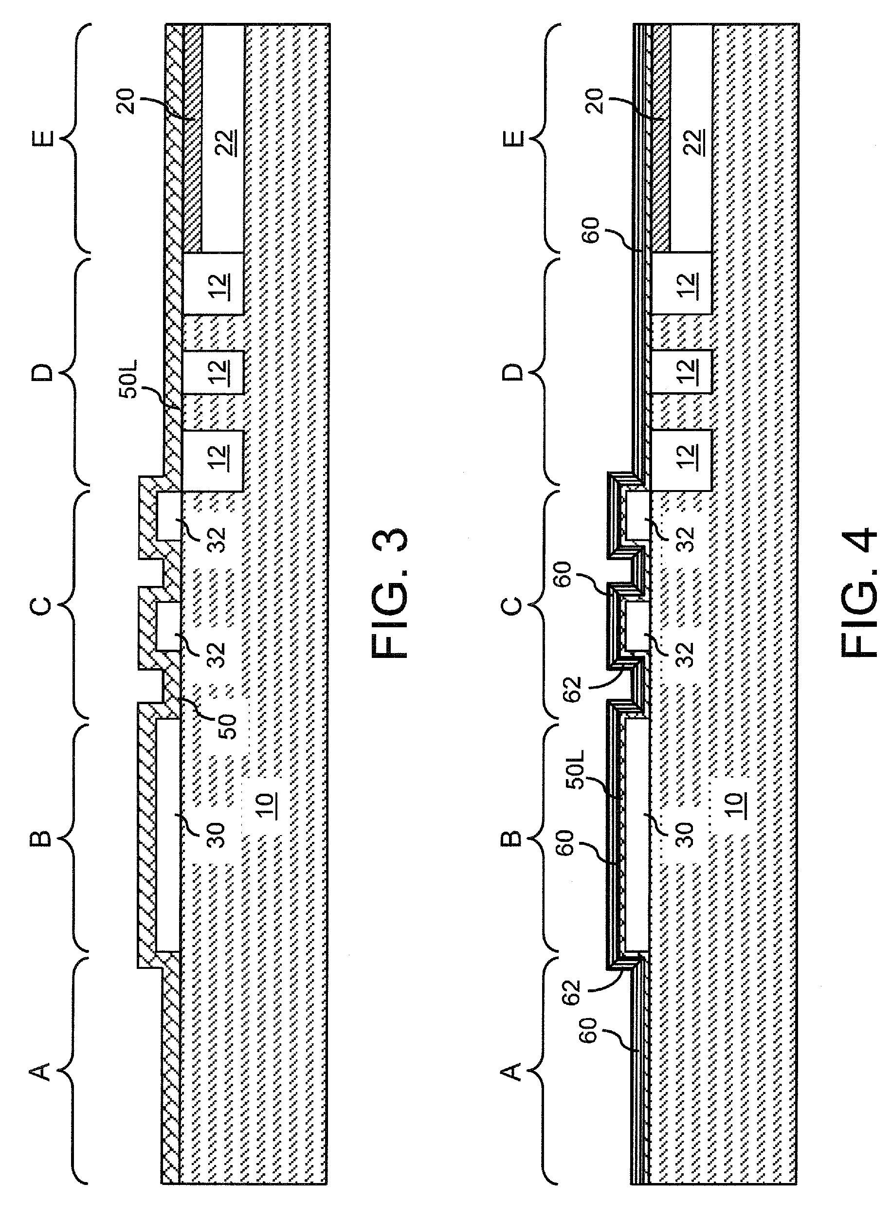
[0019]Referring to FIG. 1, a semiconductor structure according to the present invention is shown. The semiconductor substrate 10 includes a semiconductor material including silicon. The semiconductor substrate 10 may be a commercially available semiconductor substrate having a diameter from 150 mm to 300 mm, and preferably from 200 mm to 300 mm, and having a thickness from 500 micron to 1.0 mm. Preferably, the semiconductor substrate 10 is a single crystalline silicon-containing-semiconductor substrate, i.e., a single crystalline substrate containing silicon or a silicon alloy. The singe crystalline silicon-containing semiconductor substrate may include a single crystalline silicon material, a single crystalline silicon-germanium alloy material, a single crystalline silicon-carbon alloy material, or a single crystalline silicon-germanium-carbon alloy material. If the semiconductor substrate 10 is a single crystalline silicon-containing-semiconductor substrate, the semiconductor subs...
second embodiment
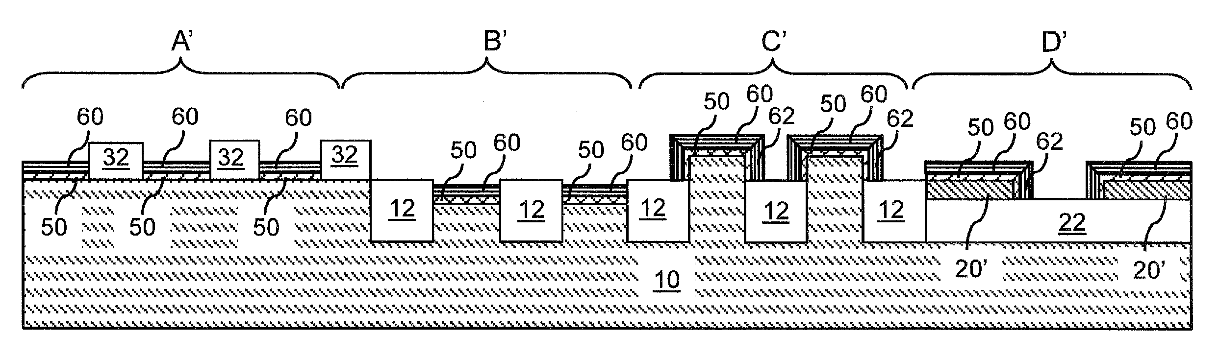
[0020]For the purpose of description of the present invention, the semiconductor substrate 10 includes a first region A having a planar exposed top surface of the semiconductor substrate 10, a second region B having an overlying dielectric material portion 30 that is located over the top surface of the semiconductor substrate 10, a third region C having patterned overlying dielectric material portions 32 that are located over the top surface of the semiconductor substrate 10, a fourth region D having exposed semiconductor surfaces of the semiconductor substrate 10 located between embedded dielectric material portions 12, and a fifth region D having a buried insulator layer 22 and a top semiconductor layer 20 having a single crystalline silicon-containing-semiconductor material. The overlying dielectric material portion 30 may be a silicon oxide layer, a silicon nitride layer, or a combination thereof. The patterned overlying dielectric material portions 32 may be portions of a silic...
PUM
| Property | Measurement | Unit |
|---|---|---|
| thickness | aaaaa | aaaaa |
| temperature | aaaaa | aaaaa |
| temperature | aaaaa | aaaaa |
Abstract
Description
Claims
Application Information