Programmable antifuse transistor and method for programming thereof
a technology of programmable anti-fuse transistors and transistors, which is applied in the direction of read-only memories, instruments, and static storage, etc., can solve the problems of high production costs, no active circuits or active circuit parts can be operated during programming, and complicated production of electrically programmable anti-fuses. achieve the effect of high long-term stability
- Summary
- Abstract
- Description
- Claims
- Application Information
AI Technical Summary
Benefits of technology
Problems solved by technology
Method used
Image

Examples
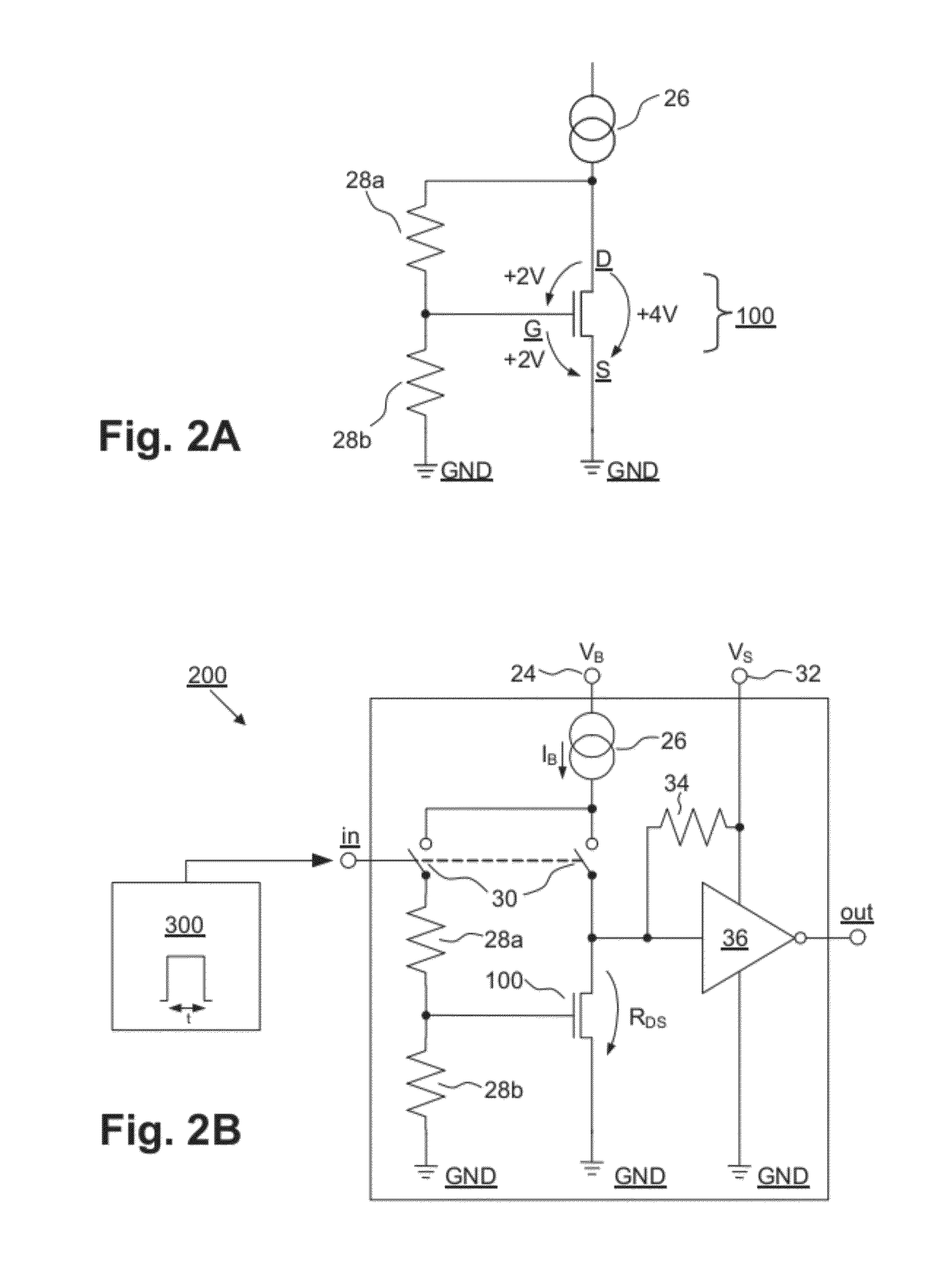
second embodiment
[0082]Correspondingly, in the antifuse circuit arrangement 200′ according to FIG. 2C[0083]in the “burnt” or “damaged” or “destroyed” state, i.e. the programmed state of the transistor 100, in view of which the voltage being fed to the input of the inverter 36 (product of the drain-source resistance RDS and the current strength ISE) is smaller than the input-based switching threshold VTh of the inverter 36, a logic “1” is given at the output out of the inverter 36, by which the output terminal of the electrically programmable permanent storage cell is simultaneously given, and[0084]in the “non-burnt” (or “unburnt”) or “non-damaged” (or “undamaged”) or “non-destroyed” (or “undestroyed”) state, i.e. the non-programmed (or unprogrammed) state of the transistor 100, in view of which the voltage being fed to the input of the inverter 36 (product of the drain-source resistance RDS and the current strength ISE) is greater than the input-based switching threshold VTh of the inverter 36, a lo...
first embodiment
[0093]200 antifuse circuit arrangement, in particular one-time electrically programmable permanent storage cell (=first embodiment; cf. FIGS. 2A, 2B)
[0094]200′ antifuse circuit arrangement, in particular one-time electrically programmable permanent storage cell (=second embodiment; cf. FIG. 2C)
[0095]300 control unit, in particular programming controller
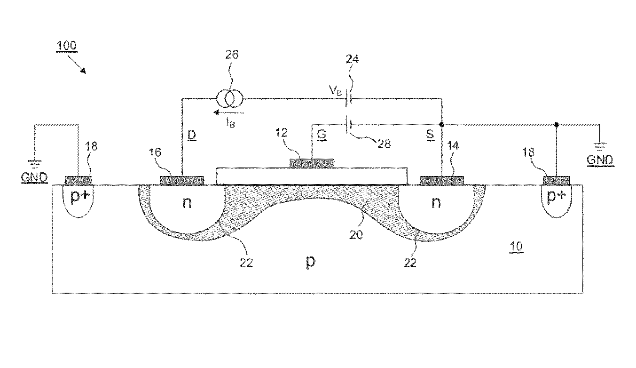
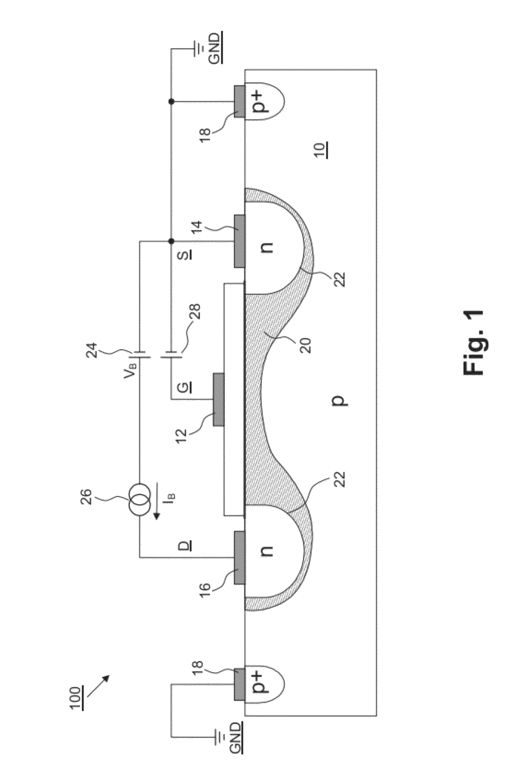
[0096]10 substrate (corresponding to base), in particular p substrate
[0097]12 terminal of the gate G, in particular gate contact or gate terminal
[0098]14 terminal of the source S, in particular source contact or source terminal
[0099]16 terminal of the drain D, in particular drain contact or drain terminal
[0100]18 terminal of the substrate 10, in particular substrate contact or substrate terminal
[0101]20 semiconductor material, in particular meltable or melted semiconductor material
[0102]22 pn junction, in particular silicon pn junction
[0103]24 voltage source, in particular burning or melting voltage source for providing the burning or...
PUM
 Abstract
Description
Claims
Application Information