Solid-state imaging apparatus and imaging system

a technology of solid-state imaging and imaging system, which is applied in the field of solid-state imaging apparatus, can solve the problems of increasing the relative accuracy of the capacitor elements, causing differential linear errors, and deteriorating the accuracy so as to reduce the deterioration of the a/d conversion accuracy, the linearity of the a/d converter can be heightened, and the resolution of the a/d converter is enhanced

Inactive Publication Date: 2012-06-26
CANON KK
View PDF50 Cites 27 Cited by
  • Summary
  • Abstract
  • Description
  • Claims
  • Application Information

AI Technical Summary

Benefits of technology

[0010]According to the present invention, the accuracy of the linearity of the A / D converter can be heightened, and can reduce the deterioration of the accuracy of the A / D conversion of the A / D converter owing to the influence of an offset even if the resolution of the A / D converter is heightened.

Problems solved by technology

However, following problem occurs when the A / D converter disclosed in Japanese Patent Application Laid-Open No. 2002-232291 is used as a column A / D.
If there is a discrepancy in a ratio of a changing quantity of an electric charge held in a capacitor per clock for a higher order bit conversion (unit integration quantity for the higher order bit conversion) to a changing quantity of an electric charge held in the capacitor per clock for a lower order bit conversion (unit integration quantity for the lower order bit conversion), a differential linear error is caused.
For example, if 12 bits A / D conversion is performed in stages of higher order digits of 6 bits and lower order digits of 6 bits, the unit integration quantity for the higher order bit conversion is ideally required to be 64 times as large as the unit integration quantity for the lower order bit conversion, but an error is caused owing to the relative accuracy of the elements constituting the circuit and the like in the actual circuit.
In particular, if the column widths of a pixel arrangement are reduced in association with the reduction of pixel sizes, then the sizes of the capacitor elements able to implement within the columns, that is, capacitor values, become smaller, and consequently the relative accuracy of the capacitor elements generally become worse.
This causes the problem in which linearity correction processing becomes a very large load especially in the case where the number of conversion bits increase.
However, in an actual circuit, the two input terminals of the operational amplifier Amp have different electric potential since the characteristics of the elements constituting the operational amplifier Amp are not necessarily ideal.
That is, the ideal integration is not performed due to the offset caused by the elements constituting the operational amplifier Amp.
However, if the resolution becomes higher, the discrepancy from the ideal value becomes nonnegligible, and the problem that the accurate A / D conversion results cannot be obtained is caused.

Method used


Image

  • Solid-state imaging apparatus and imaging system
  • Solid-state imaging apparatus and imaging system
  • Solid-state imaging apparatus and imaging system

Examples


first embodiment

[0023]A solid-state imaging apparatus according to a first embodiment, to which the present invention can be applied will be described with reference to the attached drawings.

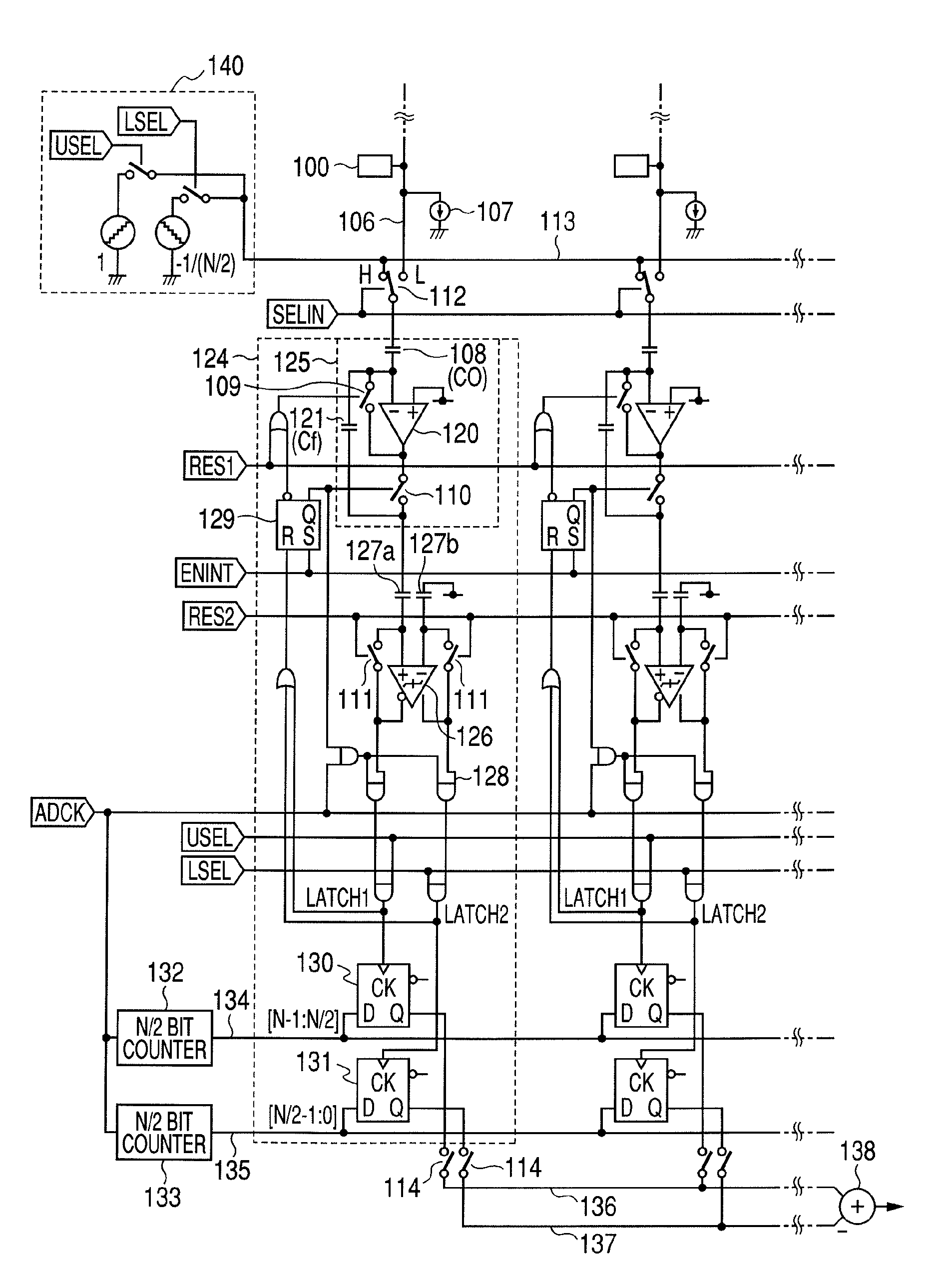
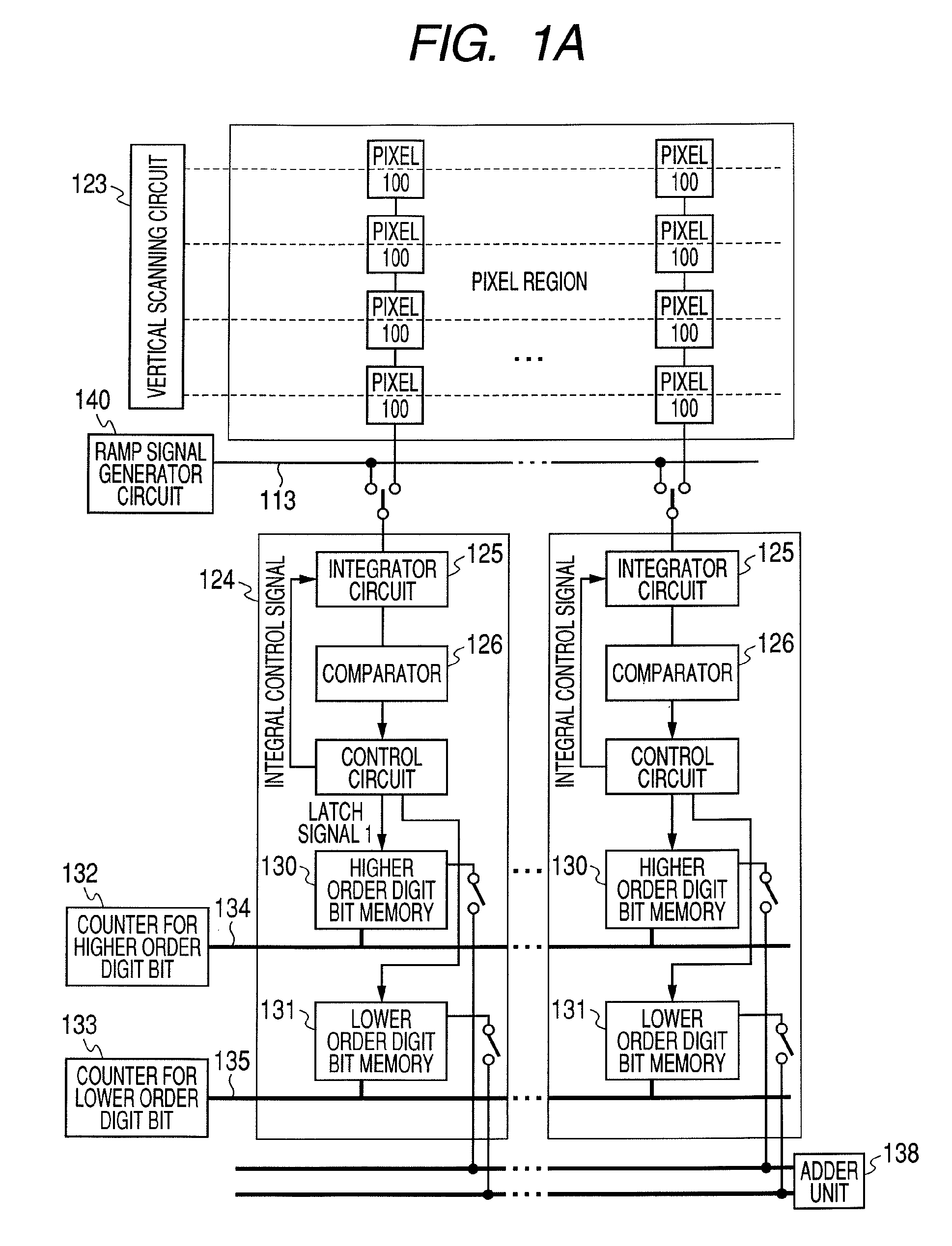
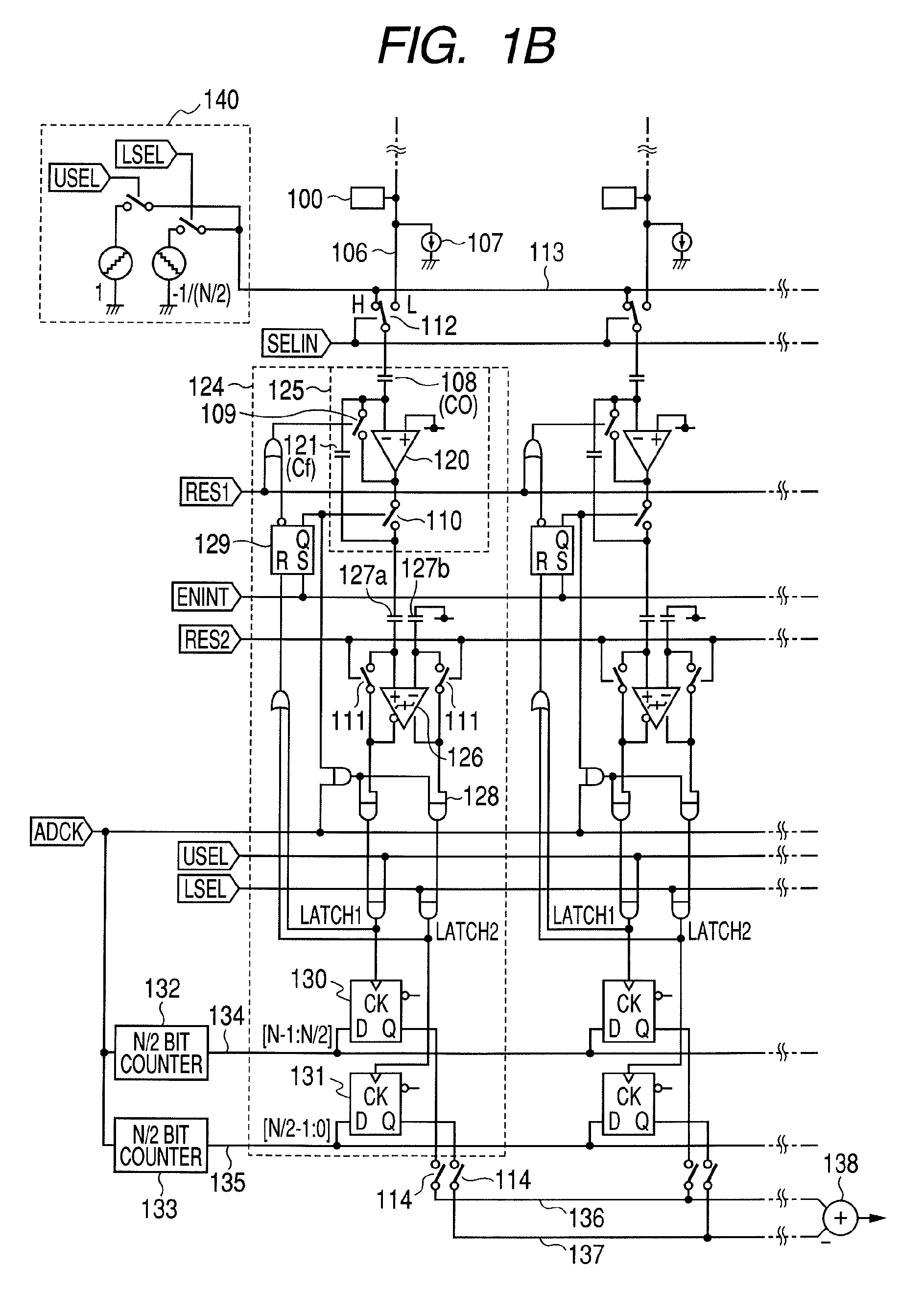
[0024]First, the outline of the solid-state imaging apparatus according to the present embodiment is described with reference to the block diagram of FIG. 1A. The solid-state imaging apparatus 1 includes a pixel region, in which a plurality of pixels 100 are arranged in a matrix, and the pixels 100 each has the configuration illustrated by the equivalent circuit of FIG. 2. Signals output from the pixels 100 are input to column read out circuits 124 provided in respective columns as analog signals through vertical output lines 106. Each of the plurality of column read out circuits 124 includes an A / D conversion circuit including an integrator circuit 125 and a comparator 126, and memories 130 and 131 storing the A / D conversion results of higher order bits and the A / D conversion results of lower order bits, respe...

second embodiment

[0045]A solid-state imaging apparatus according to a second embodiment, to which the present invention can be applied will be described with reference to FIGS. 5A AND 5B. The solid-state imaging apparatus of the present embodiment is suitable for the column A / D format of a relatively high resolution. FIG. 5A is a block diagram illustrating the outline of the solid-state imaging apparatus, and FIG. 5B illustrates a part of the equivalent circuit of the solid-state imaging apparatus. The second embodiment differs from the first embodiment in that it further comprises a measuring circuit 150 to measure a ratio of the unit integration quantity for a higher order bit conversion time period to the unit integration quantity for a lower order bit conversion time period, which ratio is determined by the reference signal generation circuit 140, and that it further comprises a correction circuit 151 to execute correction on the basis of a measured result. Furthermore, the lower order bit memor...

third embodiment

[0054]FIG. 7 is a diagram illustrating the configuration of an imaging system 1000 using the solid-state imaging apparatus of each of the aforesaid embodiments, to which the present invention is applied. 1001 denotes a barrier used as a protection of a lens and the barrier also serves as a main switch, and 1002 denotes a lens, which is an optical system for providing an optical image of a subject on a solid-state imaging apparatus 1004. The quantity of the light passing through the lens 1002 can be changed by a diaphragm 1003. The solid-state imaging apparatus 1004 (corresponding to the solid-state imaging apparatus described in each of the aforesaid embodiments) convert the optical image formed by the lens 1002 into image data. A signal processing unit 1007 performs various corrections of the image data output from the solid-state imaging apparatus 1004 and the compression of the data. A timing generator 1008 outputs various timing signals to the signal processing unit 1007. Incide...


PUM


Abstract

A solid-state imaging apparatus includes a reference signal generating circuit for supplying, commonly to the plurality of A / D conversion circuits, at least two reference signals of which signal levels change toward different directions of electric potential, and the A / D conversion circuit includes an amplifier; an input capacitor having one terminal receiving the analog signal and the reference signal supplied from the reference signal generating circuit, and the other terminal connected to one input terminal of the amplifier; a feedback capacitor connected between the one input terminal and an output terminal of the amplifier; a comparator for comparing, with a comparing level, an output from the output terminal of the amplifier; and a connection capacitor having one terminal connected to the output terminal of the amplifier, and the other terminal connected to one input terminal of the comparator.

Description

TECHNICAL FIELD[0001]The present invention relates to a solid-state imaging apparatus to be used for a scanner, a video camera, a digital still camera, and the like.BACKGROUND ART[0002]In recent years, a CMOS image sensor has been widely used for a digital camera, a digital camcorder, a camera unit for a portable telephone, and the like. Owing to the requirements of the reduction of the number of parts, the reduction of power consumption, and the like, a CMOS image sensor incorporating A / D conversion circuits has been researched. As a format of the CMOS image sensor, there is a format called a column A / D providing an A / D conversion circuit to each column of a pixel arrangement. Various A / D conversion formats have been proposed to be used for the column A / D, and among them integration type A / D conversion formats disclosed in Japanese Patent Application Laid-Open Publications No. 2002-232291 and No. 2005-348325 are known. If conversions are performed in two stages of higher order bits...

Claims


Application Information

Patent Timeline
Patent Type & Authority Patents(United States)
IPC IPC(8): H04N5/335H04N5/228H01L27/146H04N5/374H04N5/378
CPCH03M1/06H03M1/123H03M1/162H03M1/56
Inventor HIYAMA, HIROKI
Owner CANON KK
Why Eureka
Try Eureka