Solid-state image pickup device and a method of manufacturing the same

a pickup device and solid-state technology, applied in semiconductor devices, semiconductor/solid-state device details, electrical devices, etc., can solve the problems of complicated manufacturing processes, simplify the steps of forming the contact portion, reduce the element area, and simplify the manufacturing process

a pickup device and solid-state technology, applied in semiconductor devices, semiconductor/solid-state device details, electrical devices, etc., can solve the problems of complicated manufacturing processes, simplify the steps of forming the contact portion, reduce the element area, and simplify the manufacturing process

US8247306B2Inactive Publication Date: 2012-08-21SONY SEMICON SOLUTIONS CORP

Image

  • Solid-state image pickup device and a method of manufacturing the same
  • Solid-state image pickup device and a method of manufacturing the same
  • Solid-state image pickup device and a method of manufacturing the same

Examples


first embodiment

Change of First Embodiment

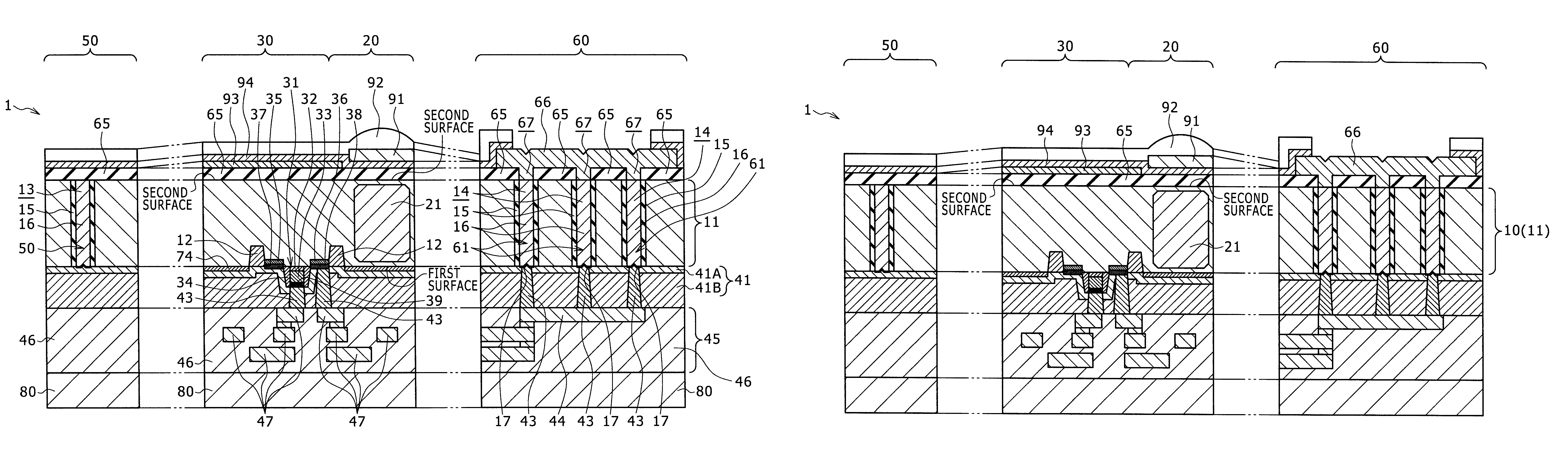
[0085]Next, a structure of a solid-state image pickup device according to a change of the first embodiment of the present invention will be described.

[0086]The solid-state image pickup device of the change of the first embodiment is such that in the solid-state image pickup device 1 of the first embodiment described with reference to FIG. 1, the silicide layer is not formed, but each of the conductive layers 16 is made of a metal. Copper (Cu), aluminum (Al), tungsten (W), titanium (Ti), tantalum (Ta) or the like, for example, can be used as this metal. In addition, an alloy thereof can also be used as this metal. It should be noted that the constituent elements other than the silicide layer and the conductive layers 16 are identical to those in the solid-state image pickup device 1 of the first embodiment.

[0087]Each of the conductive layers 16 is made of the metal in such a manner, thereby making it possible to further reduce the contact resistance between ...

second embodiment

Change of Second Embodiment

[0142]Next, a method of manufacturing a solid-state image pickup device according to a change of the second embodiment will be described.

[0143]The method of manufacturing a solid-state image pickup device according to the change of the second embodiment is such that in the method of manufacturing the solid-state image pickup device 1 described with reference to FIGS. 2 to 11, each of the conductive layers 16 is made of a metal, and the silicide layer is formed on none of the surfaces of the conductive layers 16. Copper (Cu), aluminum (Al), tungsten (W), titanium (Ti), tantalum (Ta) or the like, for example, can be used as this metal. In addition, an alloy thereof can also be used as this metal. Moreover, the manufacturing processes other than making each of the conductive layers 16 of the metal, and forming the silicide layer on none of the surfaces of the conductive layers 16 are identical to the method of manufacturing the solid-state image pickup device...


PUM


Abstract

A solid-state image pickup device includes: a silicon layer; a pixel portion formed in the silicon layer for processing and outputting signal charges obtained by carrying out photoelectric conversion for incident lights; an alignment mark formed in a periphery of the pixel portion and in the silicon layer; and a contact portion through which a first electrode within a wiring layer formed on a first surface of the silicon layer, and a second electrode formed on a second surface opposite to the first surface of the silicon layer through an insulating film are connected, wherein the alignment mark and the contact portion are formed from conductive layers made of the same conductive material and formed within respective holes each extending completely through the silicon layer through respective insulating layers made of the same material.

Description

[0001]The present application claims priority to Japanese Patent Application JP 2009-057485 filed in the Japan Patent Office on Mar. 11, 2009, the entire content of which is hereby incorporated by reference.BACKGROUND OF THE INVENTION[0002]1. Field of the Invention[0003]The present invention relates to a solid-state image pickup device, and a method of manufacturing the same.[0004]2. Description of the Related Art[0005]An example of a CMOS (Complementary Metal Oxide Semiconductor) type solid-state image pickup element to which a back surface radiation type structure to which a light is made incident from a side opposite to a side having wiring layers formed thereon to be received is applied will now be described with reference to a schematic structural cross sectional view shown in FIG. 24.[0006]As shown in FIG. 24, photodiodes PDs composing light receiving sensor portions of respective pixels are formed in a single-crystalline silicon layer 361. Also, a color filter layer 364 and l...

Claims


Application Information

Patent Timeline
21 Aug 2012
Publication
US8247306B2
IPC
H01L21/76
CPC
H01L27/14632; H01L27/14687; H01L27/14689; H01L27/1464; H01L27/14636; Y10S438/975; H01L2924/0002; H01L2924/00
Inventors
NAKAZAWA, KEIICHI; ENOMOTO, TAKAYUKI