Single heterojunction back contact solar cell

a solar cell and back contact technology, applied in the field of single heterojunction back contact solar cells, can solve the problems of high cost of single-crystal bulk silicon fabrication processes, limited cell ar, rear surface recombination loss, etc., and achieve the effect of low manufacturing cost and higher efficiency

Active Publication Date: 2012-10-16
SHARP KK
View PDF4 Cites 14 Cited by
  • Summary
  • Abstract
  • Description
  • Claims
  • Application Information

AI Technical Summary

Benefits of technology

[0017]Disclosed herein is a single heterojunction back contact solar cell. The heterojunction is formed at only one junction: either at the emitter junction or at the base junction. The other junction is formed using conventional dopant diffusion. Although the VOC for this structure is not as high as that of the double heterojunction solar cell, it has lower manufacturing cost than the double heterojunction back contact cell, and has higher efficiency than the conventional back contact cell. In addition, the anomalous “S” shaped I-V characteristic associated with the double heterojunction back contact cell is eliminated.
[0018]For example, the single heterojunction back contact cell may be fabricated on an n-type single crystal silicon (c-Si) wafer with an n+ amorphous Si (α-Si) used to form the heterojunction to c-Si at the base junction. The general consensus concerning the a-Si to c-Si heterojunction is that the valence band offset is lager than the conduction band offset. Unlike the double heterojunction cell, where both junctions hinder the minority carrier hole movement, the cell with the single heterojunction at the base only hinders the hole movement toward the base (n+) direction. This effectively reduces the carrier recombination at the base junction. The minority carriers (holes) can be collected by the emitter (p+) without “seeing” the potential barrier. Therefore, the “S” shaped I-V characteristic is eliminated.

Problems solved by technology

The limitations of this cell are
(d) rear surface recombination loss due to the low Al back surface passivation quality.
Single-crystal bulk silicon fabrication processes are expensive.
When a heterojunction is used as the base-emitter junction of a bipolar junction transistor, extremely high forward gain and low reverse gain result.
While several papers discuss a double heterojunction back contact solar cell, no simple and inexpensive means have been reported for integrating n-type α-Si and p-type α-Si on a single side of a solar cell.
The band offset may impose potential barriers for transport of photogenerated carriers across the heterojunction, thereby affecting the fill factor.

Method used


Image

  • Single heterojunction back contact solar cell
  • Single heterojunction back contact solar cell
  • Single heterojunction back contact solar cell

Examples


Embodiment Construction

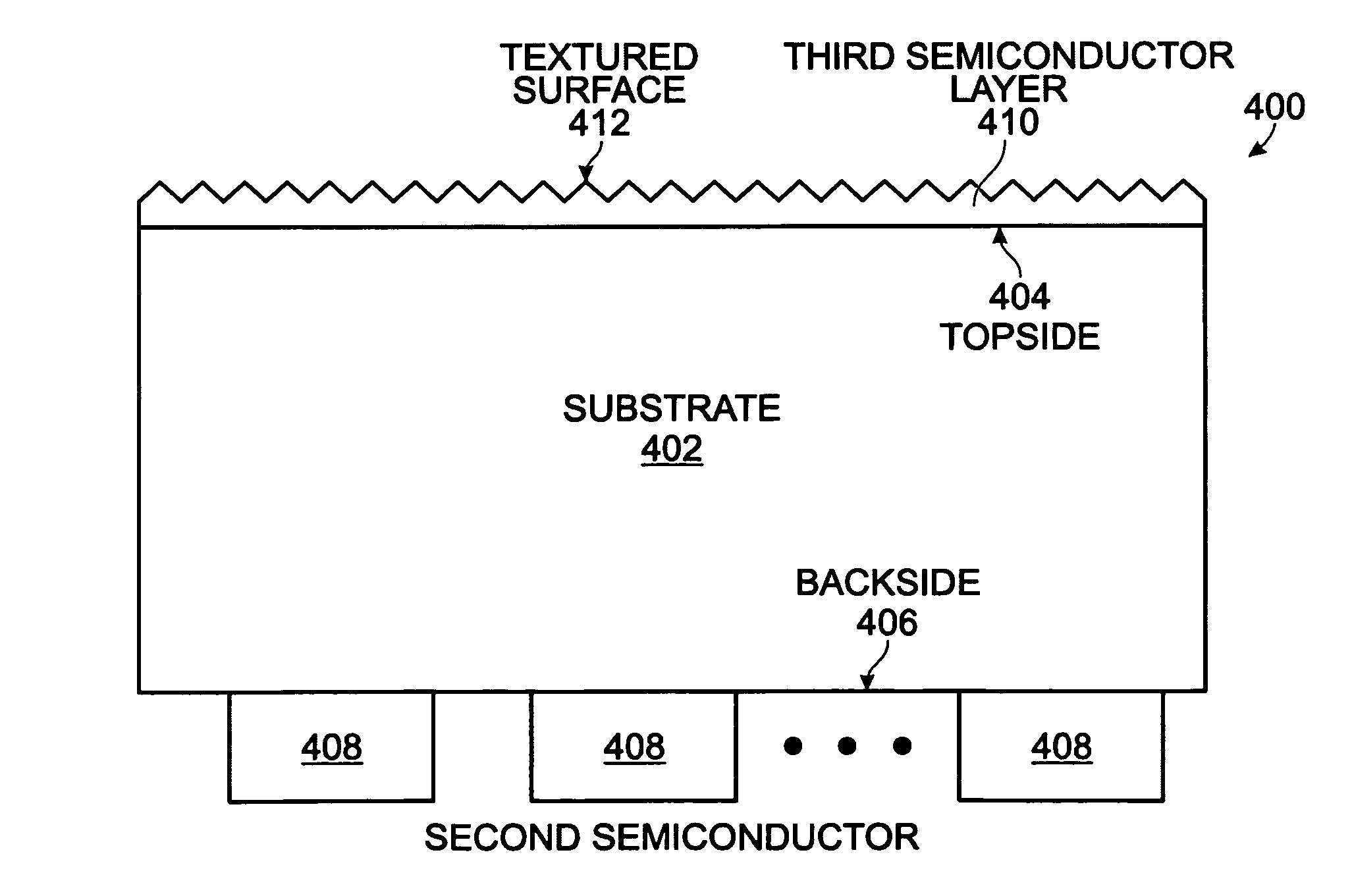
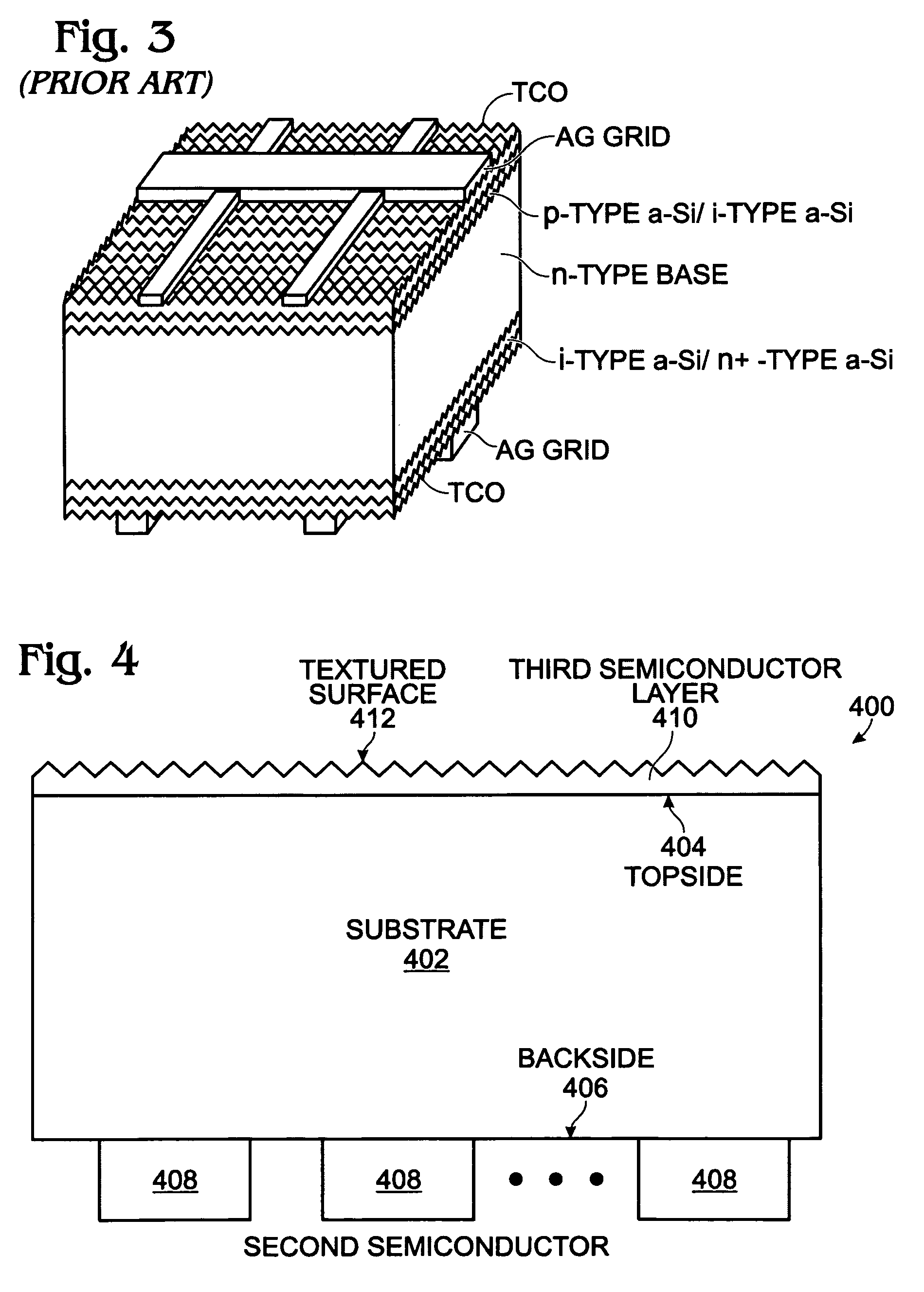
[0029]FIG. 4 is a partial cross-sectional view of a back contact single heterojunction solar cell. The solar cell 400 comprises a first semiconductor substrate 402 lightly doped with a first dopant type. The substrate 402 has a topside 404, a backside 406, and a first energy bandgap (associated with the choice of material and the doping). A second semiconductor film 408 overlies a region of the substrate backside 406. The second semiconductor 408 has a second energy bandgap, larger than the first energy bandgap. A third semiconductor layer 410 has a textured top surface 412, overlying the first semiconductor substrate topside, and is moderately doped with the first dopant.

[0030]Either the emitter or the base is formed in the second semiconductor film 408. If the emitter is formed in the second semiconductor layer (as in FIG. 5B), then the base is formed in the substrate. Alternately (as shown in FIG. 5A), if the base is formed in the second semiconductor film 408, the emitter is for...


PUM


Abstract

A back contact single heterojunction solar cell and associated fabrication process are provided. A first semiconductor substrate is provided, lightly doped with a first dopant type. The substrate has a first energy bandgap. A second semiconductor is formed over a region of the substrate backside. The second semiconductor has a second energy bandgap, larger than the first energy bandgap. A third semiconductor layer is formed over the first semiconductor substrate topside, moderately doped with the first dopant and textured. An emitter is formed in the substrate backside, heavily doped with a second dopant type, opposite of the first dopant type, and a base is formed in the substrate backside, heavily doped with the first dopant type. Electrical contacts are made to the base and emitter. Either the emitter or base is formed in the second semiconductor.

Description

BACKGROUND OF THE INVENTION[0001]1. Field of the Invention[0002]This invention generally relates to solar cell fabrication and, more particularly, to a single heterojunction back contact solar cell and associated fabrication process.[0003]2. Description of the Related Art[0004]FIG. 1 is a partial cross-sectional view of a conventional silicon solar cell (prior art). The starting silicon wafer is usually lightly boron (p) doped. The emitter layer is formed by phosphorous (n) diffusion on the wafer front surface, and the back surface field is formed by either boron diffusion or by silicon-aluminum (Si—Al) eutectic formation. The front surface has antireflection coating (ARC) and surface texturing to reduce the light reflection and improve the cell efficiency. The front grid contacts the emitter layer (n-doped region) and the back metal contacts the back surface field (p-doped) region. The limitations of this cell are[0005](a) shading loss due to the metal grid;[0006](b) series resista...

Claims


Application Information

Patent Timeline
Patent Type & Authority Patents(United States)
IPC IPC(8): H01L31/00H01L21/306
CPCH01L31/022441H01L31/02363H01L31/0682H01L31/073H01L31/0735H01L31/0747H01L31/1828H01L31/184Y02E10/543Y02E10/544Y02E10/549Y02E10/547Y02E10/546
Inventor LEE, JONG-JANSCHUELE, PAUL J.DROES, STEVEN R.
Owner SHARP KK
Why Eureka
Try Eureka