Eureka AIR delivers breakthrough ideas for toughest innovation challenges, trusted by R&D personnel around the world.

Semiconductor device

a technology of semiconductor devices and dielectric devices, applied in semiconductor devices, semiconductor/solid-state device details, capacitors, etc., can solve the problems of reduced contact resistance, inflexible control of work functions, and inability to realize low contact resistance, so as to reduce power consumption, suppress the generation of new resistance, and optimize the effect of effective work functions

Inactive Publication Date: 2012-10-30
KK TOSHIBA
View PDF9 Cites 15 Cited by
  • Summary
  • Abstract
  • Description
  • Claims
  • Application Information

AI Technical Summary

Benefits of technology

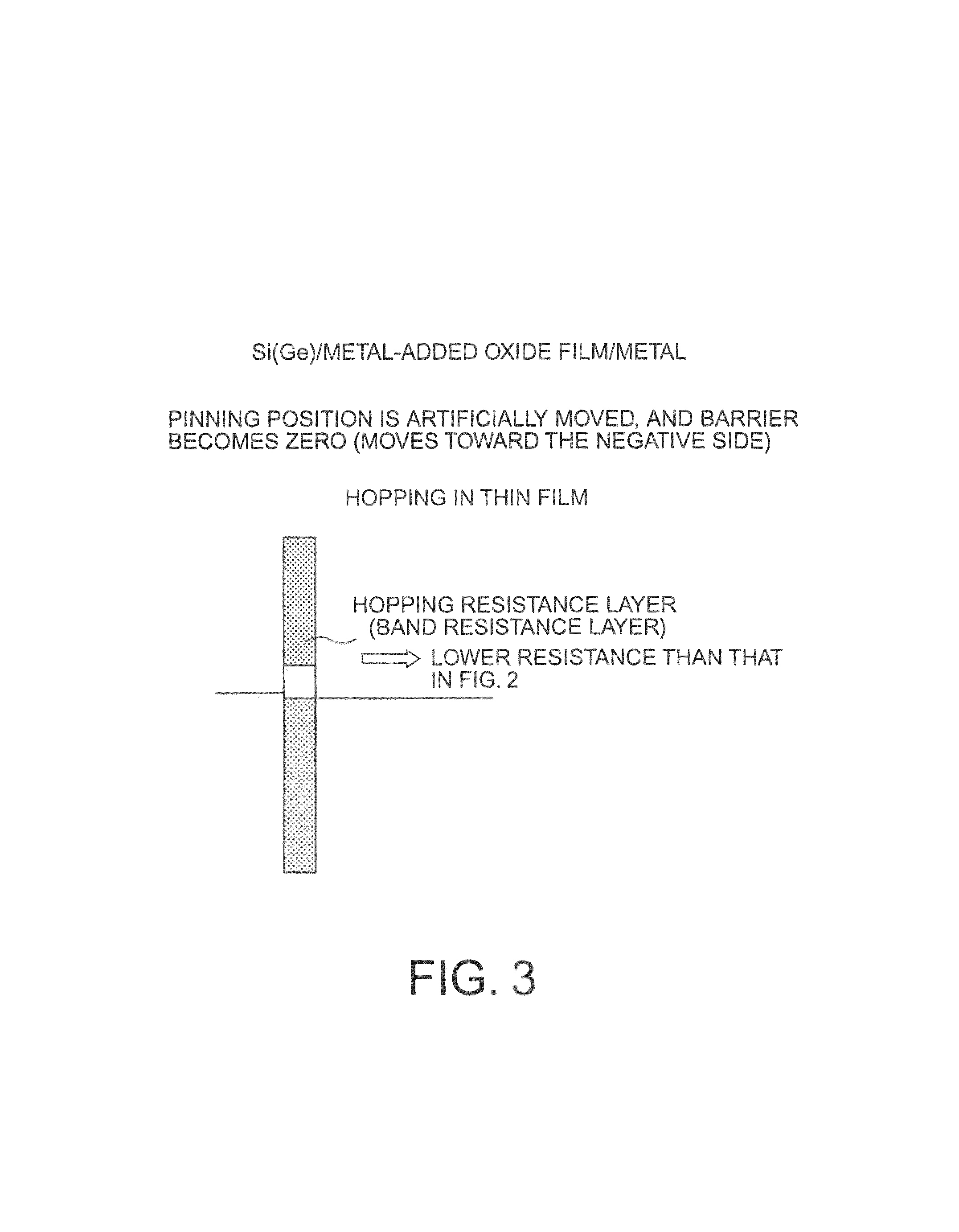
[0013]Possible embodiments of this invention are made in view of these circumstances, and some embodiments of this invention may provide a semiconductor device that can optimize the effective work function of the metal for a junction and suppress the resistance as far as possible at the interface between a semiconductor or a dielectric material and a metal.

Problems solved by technology

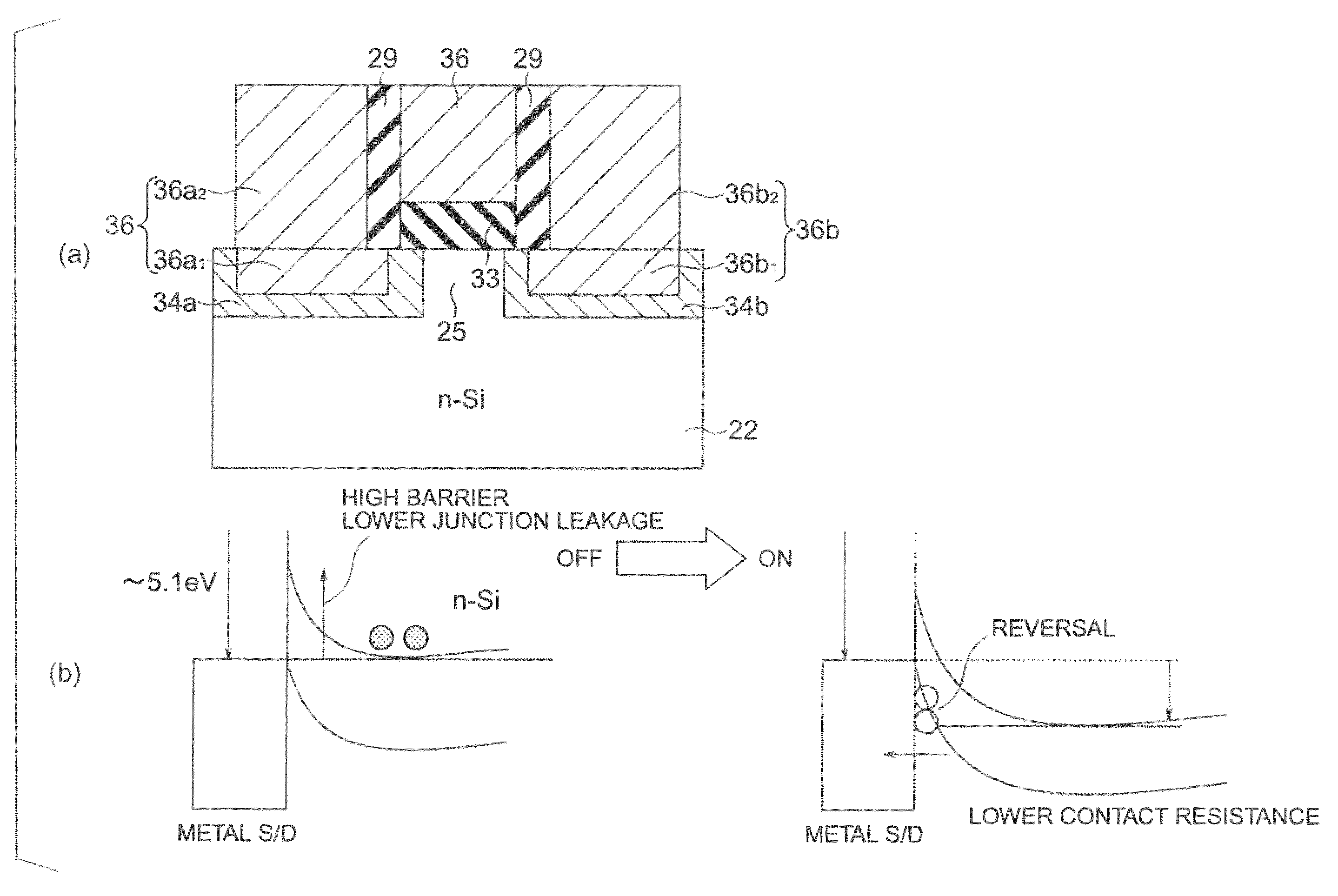
The major portion of power consumption in a MISFET (metal insulator semiconductor field effect transistor) is caused by the contact resistance between a source / drain and a metal.
In recent years, the contact resistance accounts for a large proportion of the power consumption by a MISFET, and a decrease of the contact resistance is required.
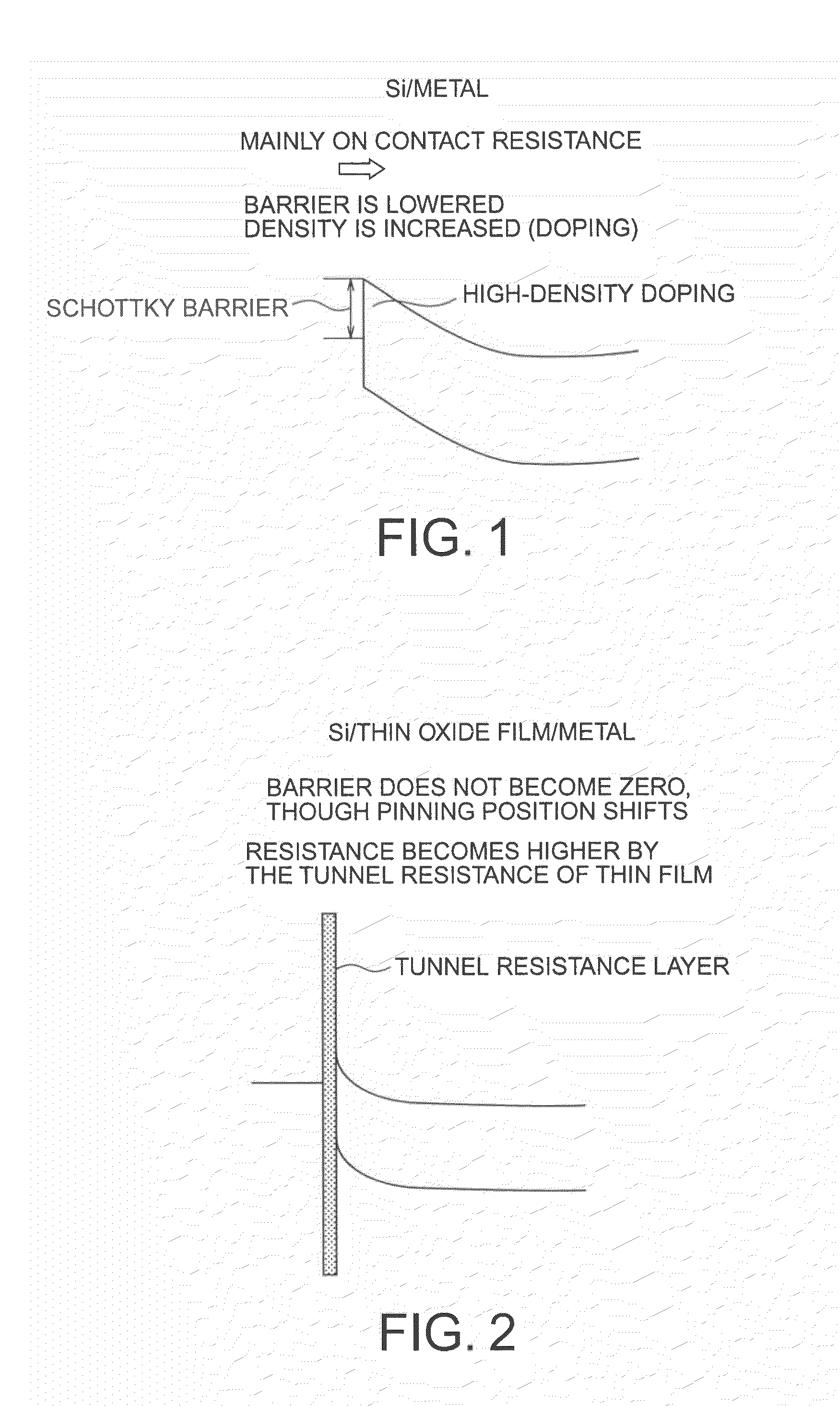
Even though the pinning by MIGS (metal induced gap states) is eliminated by the thin insulating film at the interface, the new resistance generated by the tunnel barrier is added, and because of that, realization of low contact resistance is restricted.
Furthermore, since the work function of a metal is determined by the type of the metal, the work function cannot be flexibly controlled.
As a result, an optimum work function cannot be achieved.
Therefore, there is a limit to realization of low contact resistance.
However, a high tunnel barrier is newly formed at the interface.
The first problem is that the junction effect between a semiconductor and a metal cannot be completely eliminated, and the position of pinning shifts.
Therefore, there are no measures for improvement.
The second problem is that electrons need to tunnel through an inserted insulating thin film to let current flow.
The tunnel barrier newly generates high resistance, and as a result, the power consumption becomes larger.

Method used


Image

  • Semiconductor device
  • Semiconductor device
  • Semiconductor device

Examples


example 1

Type A, n-Si

[0221]FIGS. 22(a) and 22(b) show a semiconductor device of Example 1 of the present invention. As shown in FIG. 22(a), the semiconductor device of this example has a stacked structure formed with a W-added TiO2 film 42 on an n-type silicon substrate 22, and a metal film 44 made of W and formed on the TiO2 film 42. The W added to TiO2 is an additional material of Type-A that forms a level in the band in a position higher than the bottom of the conduction band of Si when added. Through the addition of W, a junction with the n-type Si substrate without a barrier (a barrier-less junction) is formed.

[0222]The semiconductor device of this example is formed in the following manner. First, a TiO2 film is formed by sputtering on the n-type Si substrate 22, and a W film is formed by sputtering on the TiO2 film. After that, 1050° C. annealing is performed in vacuum, and 450° C. FGA (Foaming Gas Annealing) is performed in a H2 atmosphere. Through this thermal process, W diffuses int...

example 2

Type-A, n-Ge

[0251]FIGS. 25(a) and 25(b) show a semiconductor device according to Example 2 of the present invention. As shown in FIG. 25(a), the semiconductor device of this example has a stacked structure formed with a W-added TiO2 film 50 on an n-type Ge substrate 48, and a metal film 52 made of W and formed on the TiO2 film 50. The W added to TiO2 is an additional material of Type-A that forms a level in the band in a position higher than the bottom of the conduction band of Ge when added. A barrier-less junction with the n-type Ge substrate is formed.

[0252]The semiconductor device of this example is formed in the following manner. First, a TiO2 film is formed by sputtering on the n-type Ge substrate 48, and the W film 52 is formed by sputtering on the TiO2 film. The procedures to be carried out thereafter are the same as those of Example 1. The band lineup observed here is shown in FIG. 25(b). Simultaneous sputtering using the two targets of a TiO2 target and a W target is also ...

example 3

MIM Capacitor

[0276]Referring now to FIGS. 28 through 29(b), a semiconductor device of Example 3 of the present invention is described. The semiconductor device of this example is a MIM capacitor that has a stacked structure formed with a metal, an insulating material, and a metal. As shown in FIG. 28, a stacked structure is placed on a silicon substrate 60. In this stacked structure, a TiAlN buffer layer 61, a SrRuO3 electrode 62, a Mo-added TiON film (an interfacial control oxide film) 63, a Pb(Zr, TiO3 ferroelectric film 64, a Mo-added TiON film (an interfacial control oxide film) 65, and a SrRuO3 electrode 66 are stacked in this order. Each of the layers is formed by sputtering. Particularly, the Mo-added TiON films 63 and 65 are formed in an Ar / O2 / N2 atmosphere by simultaneous sputtering using a Mo target and a TiO2 target. After all the film formation is completed, 1050° C. annealing is performed in vacuum, and 450° C. FGA (Foaming Gas Annealing) is performed in a H2 atmosphere...


PUM

PropertyMeasurementUnit
thicknessaaaaaaaaaa
thicknessaaaaaaaaaa
work functionaaaaaaaaaa

Abstract

It is made possible to optimize the effective work function of the metal for a junction and suppress the resistance as far as possible at the interface between a semiconductor or a dielectric material and a metal. A semiconductor device includes: a semiconductor film; a Ti oxide film formed on the semiconductor film, and including at least one element selected from the group consisting of V, Cr, Mn, Fe, Co, Ni, Nb, Mo, Tc, Ru, Rh, Pd, Ta, W, Re, Os, Ir, and Pt; and a metal film formed on the Ti oxide film.

Description

CROSS-REFERENCE TO RELATED APPLICATION[0001]This application is based upon and claims the benefit of priority from prior Japanese Patent Application No. 2009-55183 filed on Mar. 9, 2009 in Japan, the entire contents of which are incorporated herein by reference.BACKGROUND[0002]1. Technical Field[0003]The present invention relates to a semiconductor device.[0004]2. Related Art[0005]The major portion of power consumption in a MISFET (metal insulator semiconductor field effect transistor) is caused by the contact resistance between a source / drain and a metal. This is because a Schottky barrier is formed at the interface between the semiconductor and the metal, and the barrier becomes electric resistance. In recent years, the contact resistance accounts for a large proportion of the power consumption by a MISFET, and a decrease of the contact resistance is required.[0006]To solve this problem, a thin insulating film of 2 nm or less made of silicon nitride, silicon oxide, silicon oxynitr...

Claims


Application Information

Patent Timeline
Patent Type & Authority Patents(United States)
IPC IPC(8): H01L29/78
CPCH01L21/28176H01L29/7881H01L21/28518H01L21/2855H01L21/28556H01L21/31604H01L28/75H01L29/41775H01L29/45H01L29/456H01L29/513H01L29/517H01L29/518H01L29/66545H01L29/6659H01L21/283H01L21/02192H01L21/02194H01L21/02153H01L21/02186
Inventor SHIMIZU, TATSUOKINOSHITA, ATSUHIRO
Owner KK TOSHIBA
Why Eureka
Eureka Blog
Learn More