Method of making a semiconductor chip assembly with a ceramic/metal substrate

a technology of ceramic/metal substrate and semiconductor chip, which is applied in the direction of semiconductor devices, semiconductor/solid-state device details, electrical devices, etc., can solve the problems of heat not only degrading the chip, short life span and immediate failure of the semiconductor device at high operating temperature, and easy degradation of the chip performance. , to achieve the effect of excellent heat spreading and heat dissipation, low cost and low thermal conductivity

Inactive Publication Date: 2012-11-06
BRIDGE SEMICON
View PDF87 Cites 14 Cited by
  • Summary
  • Abstract
  • Description
  • Claims
  • Application Information

AI Technical Summary

Benefits of technology

[0038]The present invention has numerous advantages. The base can provide excellent heat spreading and heat dissipation without heat flow through the insulative material. As a result, the insulative material can be a low cost dielectric with low thermal conductivity and not prone to delamination. The ceramic block can provide thermal expansion matching with a semiconductor device mounted thereon, thereby increasing reliability. The ceramic block can also electrically isolate the semiconductor device from the base, thereby providing electrostatic discharge (ESD) protection for the semiconductor device. The assembly can be manufactured using low temperature processes after the ceramic block is formed which reduces stress and improves reliability. The assembly can also be manufactured using well-controlled processes which can be easily implemented by circuit board, lead frame and tape manufacturers.

Problems solved by technology

Semiconductor devices are susceptible to performance degradation as well as short life span and immediate failure at high operating temperatures.
The heat not only degrades the chip, but also imposes thermal stress on the chip and surrounding elements due to thermal expansion mismatch.
LEDs include high power chips that generate high light output and considerable heat.
Unfortunately, LEDs exhibit color shifts and low light output as well as short lifetimes and immediate failure at high operating temperatures.
Furthermore, LED light output and reliability are constrained by heat dissipation limits.
However, since the plastic and the dielectric layer typically have low thermal conductivity, the PBGA provides poor heat dissipation.
However, since the lead frame type interposer has limited routing capability, the QFN package cannot accommodate high input / output (I / O) chips or passive elements.
Conventional packages and thermal boards have major deficiencies.
For instance, dielectrics with low thermal conductivity such as epoxy limit heat dissipation, whereas dielectrics with higher thermal conductivity such as epoxy filled with ceramic or silicon carbide have low adhesion and are prohibitively expensive for high volume manufacture.
The dielectric may delaminate during manufacture or prematurely during operation due to the heat.
The substrate may have single layer circuitry with limited routing capability or multi-layer circuitry with thick dielectric layers which reduce heat dissipation.
The heat spreader may be inefficient, cumbersome or difficult to thermally connect to the next level assembly.
The manufacturing process may be unsuitable for low cost, high volume manufacture.

Method used


Image

  • Method of making a semiconductor chip assembly with a ceramic/metal substrate
  • Method of making a semiconductor chip assembly with a ceramic/metal substrate
  • Method of making a semiconductor chip assembly with a ceramic/metal substrate

Examples


Embodiment Construction

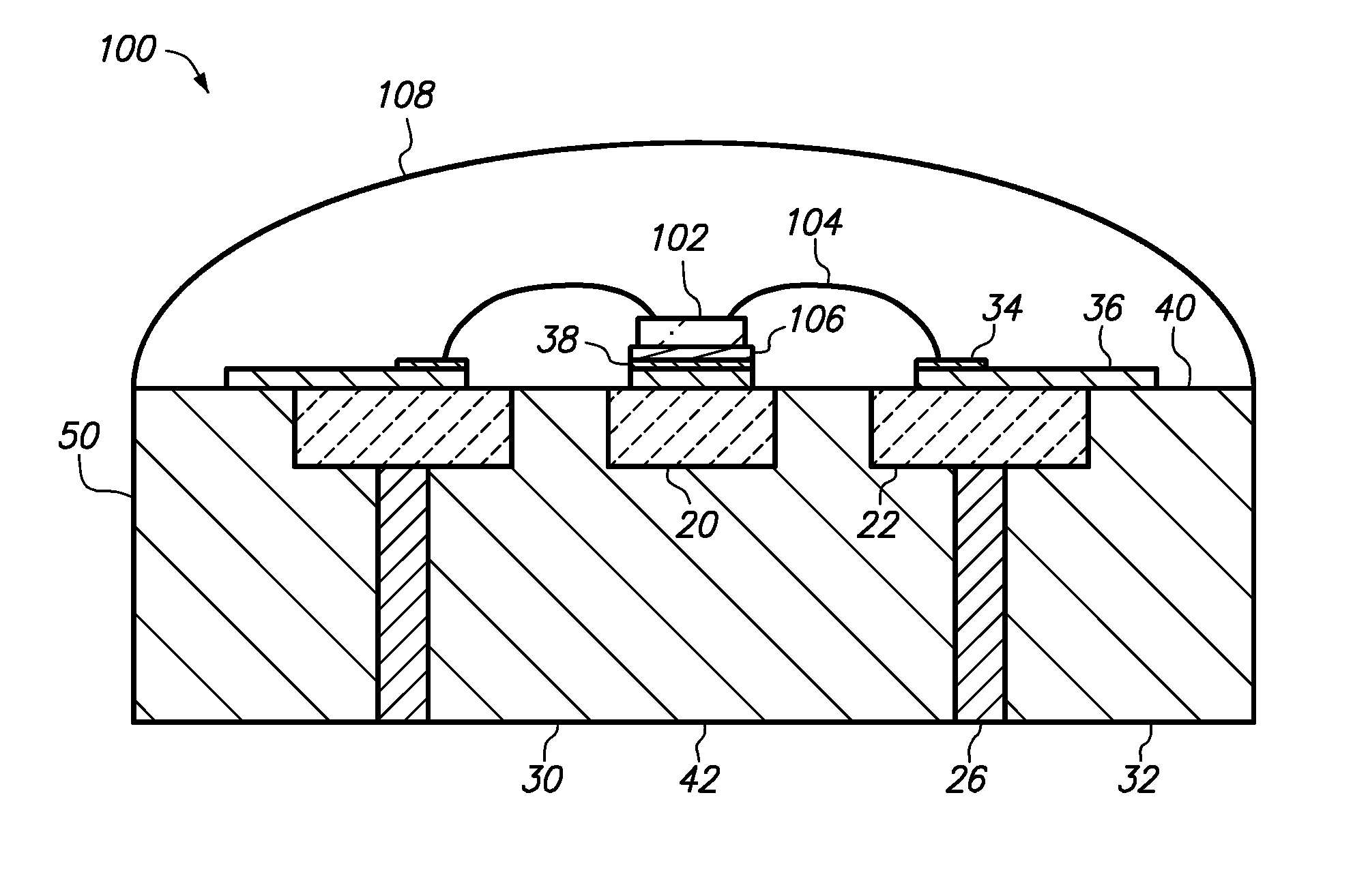
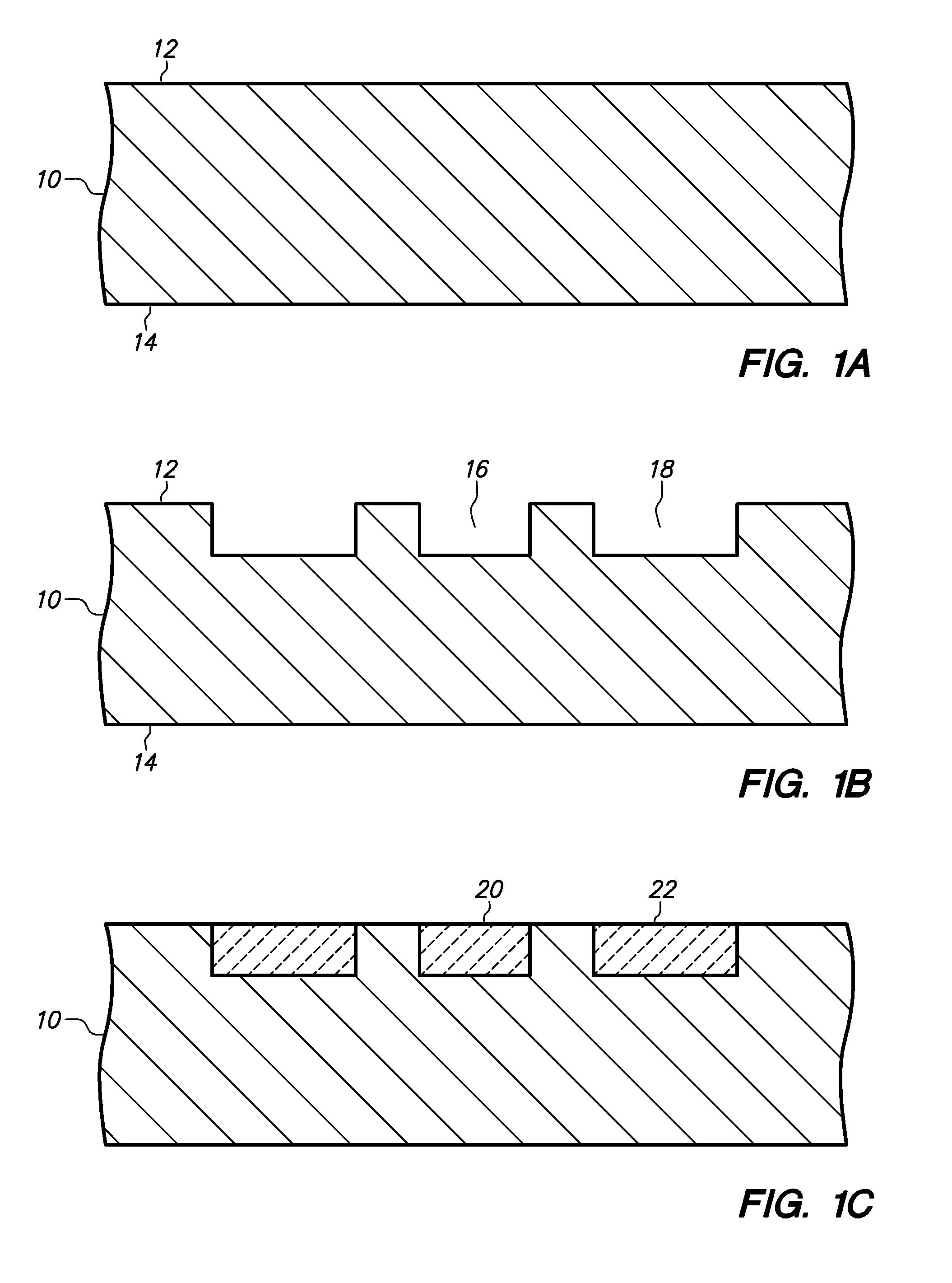
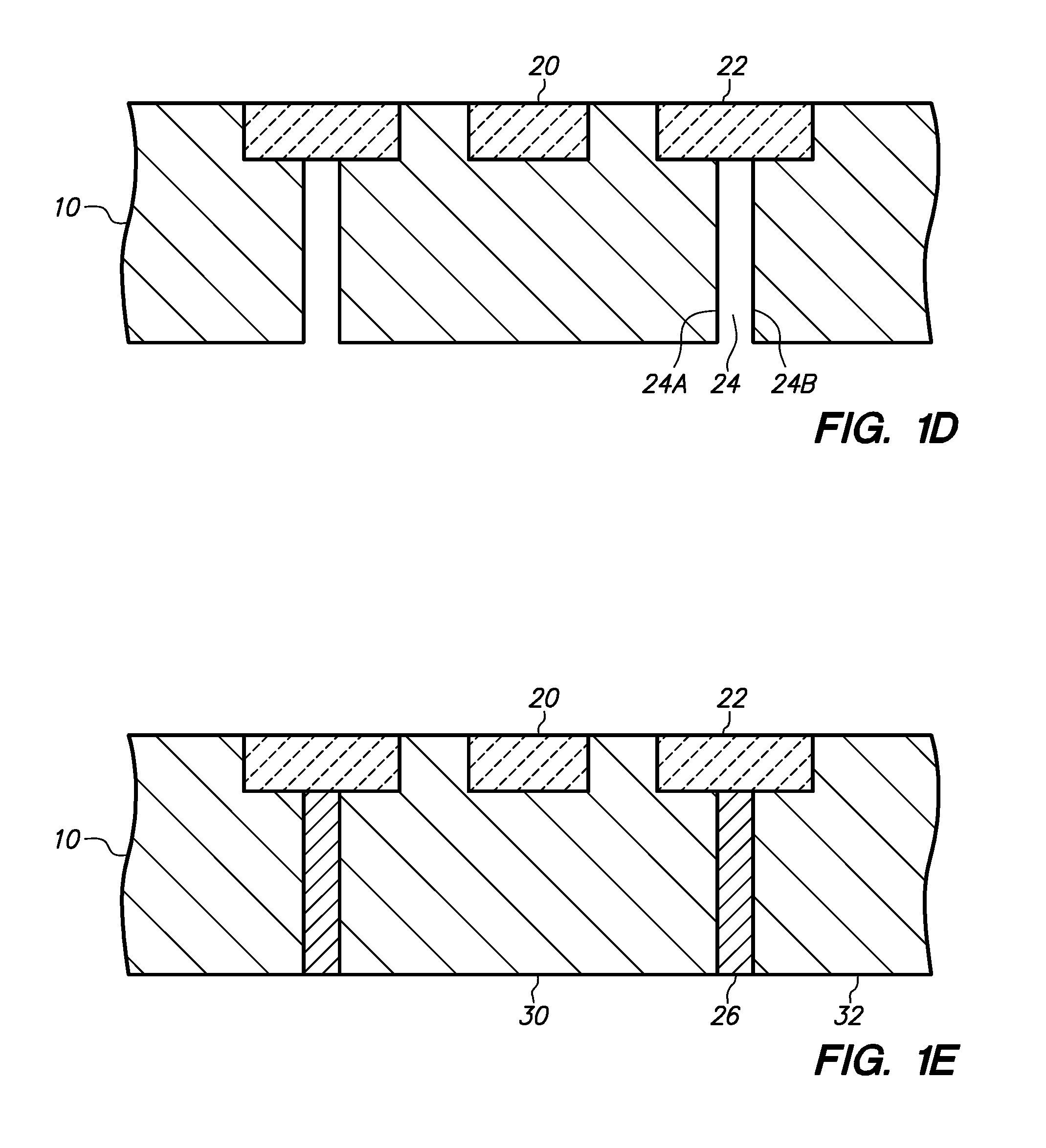
[0049]FIGS. 1A-1H are cross-sectional views showing a method of making a substrate with a ceramic block in the base and another ceramic block in the base and the terminal in accordance with an embodiment of the present invention, and FIGS. 1I and 1J are top and bottom views, respectively, corresponding to FIG. 1H.

[0050]FIG. 1A is a cross-sectional view of metal plate 10 which includes top surface 12 and bottom surface 14. Metal plate 10 is copper and has a thickness of 2000 microns.

[0051]FIG. 1B is a cross-sectional view of cavities 16 and 18 in metal plate 10. Cavities 16 and 18 extend into metal plate 10 at top surface 12, are spaced from bottom surface 14 and face in the upward direction and have a depth of 750 microns.

[0052]Cavities 16 and 18 are formed using an etch mask on top surface 12 and a cover mask on bottom surface 14. The etch mask and the cover mask are photoresist layers deposited on metal plate 10 by dry film lamination although wet spin coating and curtain coating ...


PUM

PropertyMeasurementUnit
thicknessaaaaaaaaaa
depthaaaaaaaaaa
pHaaaaaaaaaa

Abstract

A method of making a semiconductor chip assembly includes providing a metal plate, providing a ceramic block in the metal plate, providing an insulative material in the metal plate, wherein the metal plate includes a base and a terminal, then providing a conductive layer on the base and the ceramic block, providing a conductive trace that includes a pad, the terminal and a selected portion of the conductive layer, then mounting a semiconductor device on the ceramic block, wherein a heat spreader includes the base and the ceramic block, electrically connecting the semiconductor device to the conductive trace and thermally connecting the semiconductor device to the heat spreader.

Description

CROSS-REFERENCE TO RELATED APPLICATIONS[0001]This application is a divisional of U.S. application Ser. No. 12 / 848,176 filed Aug. 1, 2010, which claims the benefit of U.S. Provisional Application Ser. No. 61 / 231,686 filed Aug. 6, 2009.BACKGROUND OF THE INVENTION[0002]1. Field of the Invention[0003]The present invention relates to semiconductor chip assembly, and more particularly to a semiconductor chip assembly with a semiconductor device and a ceramic / metal substrate and its method of manufacture.[0004]2. Description of the Related Art[0005]Semiconductor devices such as packaged and unpackaged semiconductor chips have high voltage, high frequency and high performance applications that require substantial power to perform the specified functions. As the power increases, the semiconductor device generates more heat. Furthermore, the heat build-up is aggravated by higher packing density and smaller profile sizes which reduce the surface area to dissipate the heat.[0006]Semiconductor d...

Claims


Application Information

Patent Timeline
Patent Type & Authority Patents(United States)
IPC IPC(8): H01L21/50H01L21/56H01L21/58
CPCH01L23/3121H01L23/142H01L23/36H01L23/498H01L24/32H01L24/48H01L2924/01029H01L2224/73265H01L2224/85H01L2224/32245H01L2224/48227H01L2924/09701H01L2924/01028H01L2924/01014H01L2924/01013H01L2224/48091H01L2924/01322H01L2224/83H01L2924/12041H01L24/83H01L24/85H01L2224/29144H01L2224/32225H01L2224/45144H01L2924/3025H01L2924/00012H01L2924/00014H01L2924/0105H01L2924/00H01L2924/351H01L24/45H01L24/73H01L2924/181H01L2224/05599
Inventor LIN, CHARLES W. C.WANG, CHIA-CHUNG
Owner BRIDGE SEMICON
Why Eureka
Try Eureka