Memory control device, memory device, and memory control method

a control device and memory technology, applied in the direction of memory adressing/allocation/relocation, micro-instruction address formation, instruments, etc., can solve the problems of inaccessible period, inability to fully mask the inaccessible period, and inability to generate latency in the data bus, so as to suppress the increase of the minimum access unit of the memory, suppress the increase of invalid data transfer, and extend the memory bandwidth

Active Publication Date: 2012-11-06
PANASONIC CORP
View PDF30 Cites 11 Cited by
  • Summary
  • Abstract
  • Description
  • Claims
  • Application Information

AI Technical Summary

Benefits of technology

[0054]According to the memory control device of an aspect of the present invention, it is possible to suppress increase in the minimum access unit of a memory when the bus width is extended and when a high-speed DRAM such as DDR, DDR2, and DDR3 is used to extend the memory bandwidth to be used. Thus, it is possible to suppress increase in invalid data transfer in a system with small transfer amount and with random non-continuous access which frequently occurs upon image processing and achieve high access efficiency. Furthermore, it is possible to improve effective transfer efficiency by reducing unnecessary transfer, and to improve access overhead unique to the memory units (especially in DRAM), and reduces the total bandwidth of the memory system. At the same time, it is also possible to reduce the number of terminals in the system LSI and the number of wiring between the LSI and the memory units. This also achieves significant reduction in cost.
[0055]Within the aspects of the present invention, replacing the memory units having multiple chips into one memory package achieves reduction in the unnecessary transfer, improvement in the effective transfer efficiency, improvement on the access overhead specific to a memory device (especially DRAMs), reduction in the total bandwidth in the memory system, and significant reduction in the implementation area in the system by reducing the number of implemented chips in the system.

Problems solved by technology

During the activation process and the precharge process, the bank cannot be accessed, which generates an inaccessible period when switching the row in the same bank and generates latency in data bus.
As a result, even with the bank interleaving, the inaccessible period is not fully masked unless the data transfer amount to the other bank is increased, more specifically, unless the transfer size per access is increased.
Consequently, latency in the data bus is generated, and the access efficiency is reduced.
This indicates significant reduction in the access efficiency in a system where frequent access with small transfer size is performed.

Method used


Image

  • Memory control device, memory device, and memory control method
  • Memory control device, memory device, and memory control method
  • Memory control device, memory device, and memory control method

Examples


first embodiment

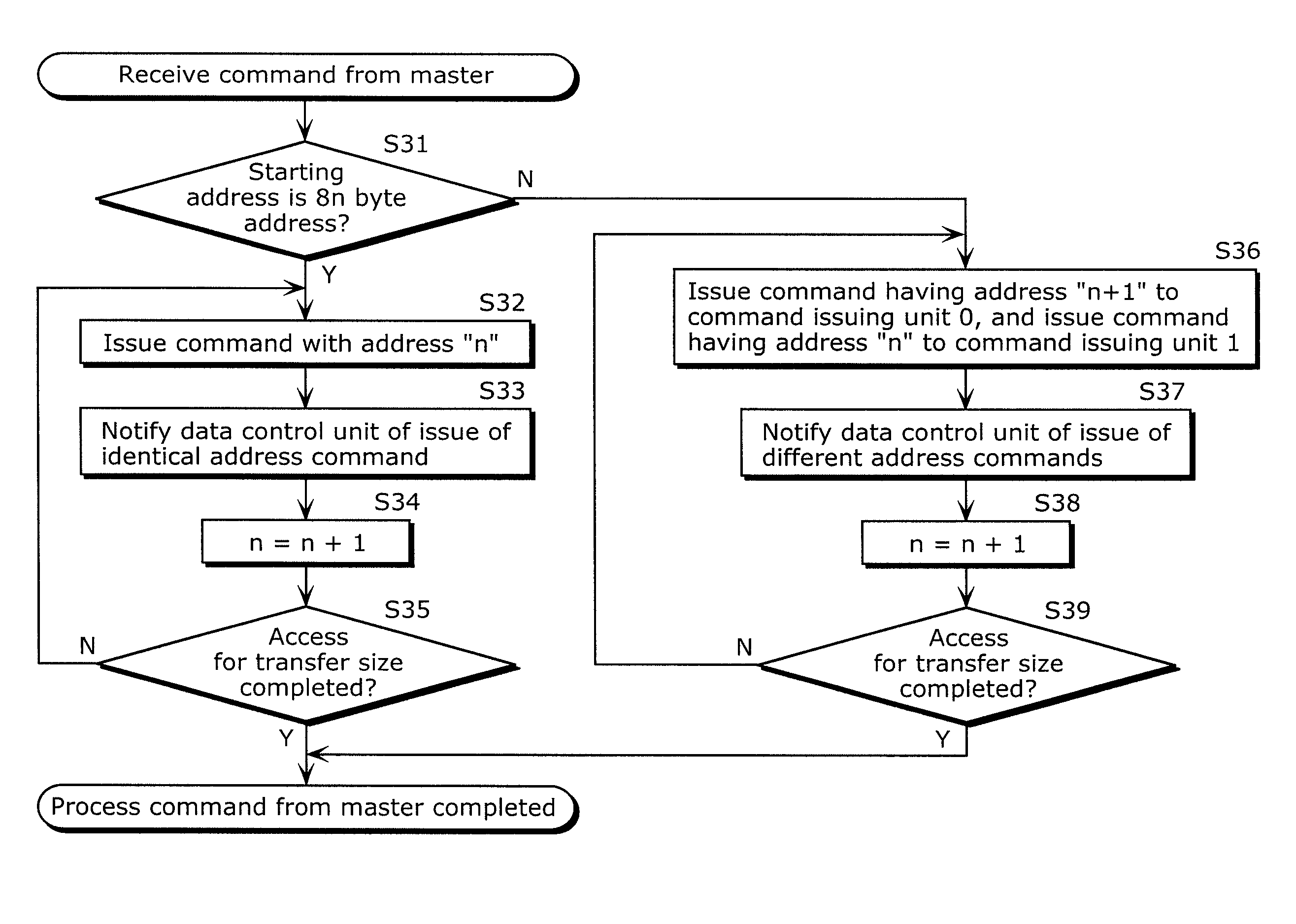
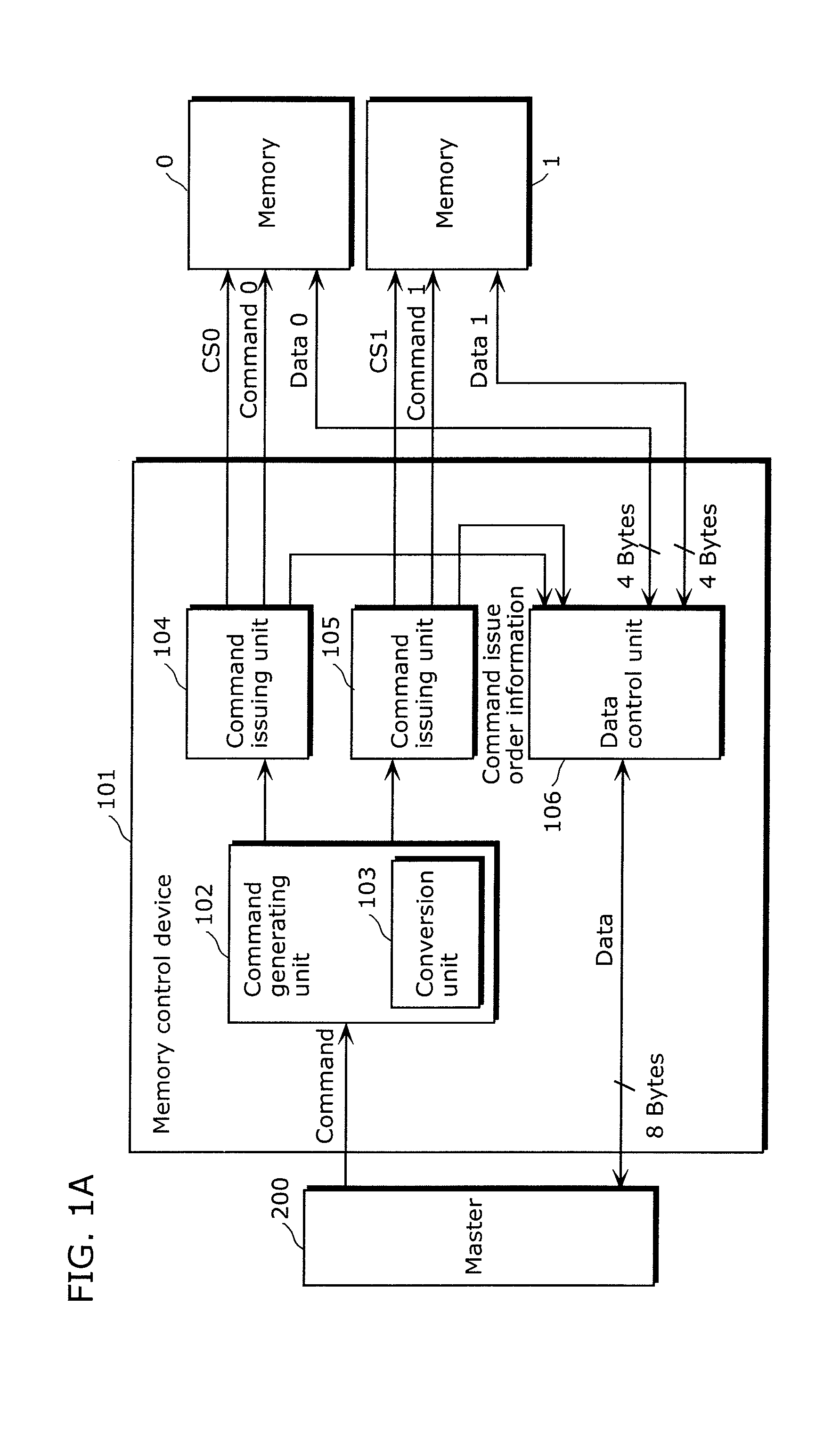
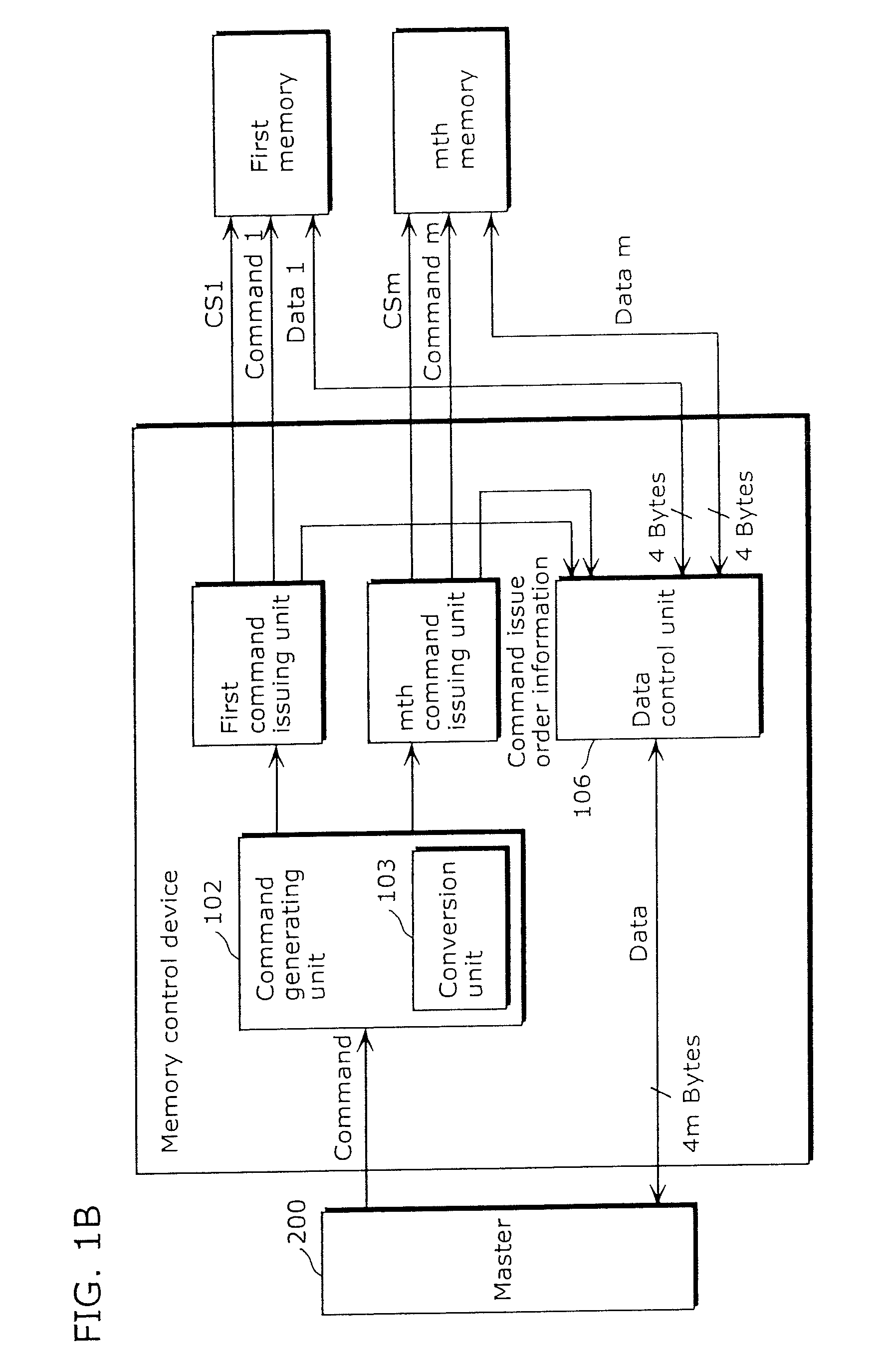
[0114]The memory control device according to the present invention includes a command control unit which divides the memory access request issued by the master into access commands each of which is for one of the memory devices, and issues each of the access commands to a corresponding one of the memory devices; and a data control unit which (i) divides data written by the master into pieces of data each of which is for one of the memory devices and outputs each piece of the divided data to the corresponding one of the memory devices, when the memory access request is a write request, and (ii) combines pieces of data read from the memory devices and outputs the combined read data to the master, when the memory access request is a read request. Here, the command control unit switches between control for outputting an identical physical address to the memory devices and control for outputting different physical addresses to the memory devices, depending on when the physical addresses ...

second embodiment

[0143]In the second embodiment, a configuration of a memory control device which allows miniaturization of the circuit by significantly reducing the wiring area of the address bus compared to the first embodiment, while the performance is not significantly deteriorated.

[0144]The command control unit in the second embodiment is connected to the memory devices via an address bus common to the memory devices and chip select signal lines individual to the memory devices. The command control unit (i) simultaneously asserts the respective chip select signals and output the identical physical address to the memory devices when the divided access commands indicate the identical physical address, and (ii) asserts the respective chip select signals at different timings and output the different physical addresses to the memory devices when the divided access commands indicate the different physical addresses. As described above, shifting the timings (for example, for 1 cycle) causes delay for ...

third embodiment

[0180]The following describes an arrangement of logical address to maximize the effect of the memory control device according to the first and second embodiments to the fullest extent.

[0181]FIG. 11A shows a unit area as base unit for mapping the physical address in the logical address space. In FIG. 11A, it is assumed that the memory control device accessing m memory devices (here, DRAMs) for example, as shown in FIG. 1B and FIG. 6B are used. FIG. 11A shows a memory address arrangement on a DRAM, and physical address area in DRAM having n-bytes minimum access unit is arranged in the direction of logical address.

[0182]In FIG. 11A, the data on the first memory device is arranged for (N×integer) bytes, and the data on the second memory device is arranged for (N×integer) bytes. After repeating this process, the data of (N×integer) bytes on the m-th memory device is adjacently arranged. As described above, the adjacent (N×integer)×m bytes of data area is considered to be one unit (unit a...


PUM


Abstract

The memory control device according to the present invention includes a command generating unit which divides the memory access request issued by the master into access commands each of which is for one of the memory devices, a command issuing units which issue each of the access commands to the memory devices, a data control unit which switches data between a master and memories, and the command generating unit switch between control for outputting an identical physical address to the memory units and control for outputting different physical addresses to the memory devices, depending on when the physical addresses of the memory devices are identical and when the physical addresses of the memory devices are different, each of the memory devices corresponds to one of the divided access commands.

Description

TECHNICAL FIELD[0001]The present invention relates to a memory control device, a memory device, and a memory control method in a system where the memory data bus width is extended to increase available memory bandwidth, for enhancing effective transfer efficiency of accesses from a master to any address.BACKGROUND ART[0002]Information processing devices including image processors generally use large-volume and low-cost DRAMs to store a large amount of data. More particularly, recent image processors require DRAMs with not just memory capacity but with high data transferring capability (hereinafter referred to as a memory bandwidth) for High Definition (HD) image processing in MPEG 2 and H.264, simultaneous multiple channel processing, and high-quality 3D graphics processing.[0003]For achieving the high memory bandwidth, some conventional methods have been generally known, including: (1) improving the operational frequency of bus; (2) allowing a wide bus width in a memory; and a meth...

Claims


Application Information

Patent Timeline
Patent Type & Authority Patents(United States)
IPC IPC(8): G06F12/00
CPCG06T1/60G06F13/1668G06F12/06G06F12/02G06T1/20
Inventor YAMADA, TAKASHIIMOTO, DAISUKEASAI, KOJIICHIGUCHI, NOBUYUKIMOCHIDA, TETSUJI
Owner PANASONIC CORP
Why Eureka
Try Eureka