Methods for improving the quality of group III-nitride materials and structures produced by the methods

a technology of group iii-nitride and methods, which is applied in the direction of basic electric elements, electrical apparatus, and semiconductor devices, can solve the problems of material density, dislocation, and difficulty in growing bulk single crystals, and achieve the effect of preventing decomposition and reducing surface defect density

Active Publication Date: 2012-11-27
SOITEC SA +1
View PDF6 Cites 3 Cited by
  • Summary
  • Abstract
  • Description
  • Claims
  • Application Information

AI Technical Summary

Benefits of technology

[0011]Preferably, the regions of amorphous complex material are formed located at or proximate to some or all of the surface emergent defects and include materials that substantially prevent the nucleation of the following Group III-nitride semiconductor material thereon. Also preferably, the regions of amorphous complex material preferably substantially prevent the propagation of defects and dislocations from the initial Group III-nitride semiconductor layer into the following Group III-nitride semiconductor layer so that the following Group III-nitride semiconductor layer thereby has a lower surface defect density then the initial Group III-nitride semiconductor layer.
[0012]In particular aspects, these methods preferably form the regions of amorphous complex material by occluding a plurality of the surface defects with a protective layer of protective material, and then by thermally treating, preferably at a temperature of at least 600° C., the initial Group III-nitride semiconductor layer with the protective layer of protective material thereon. The protective layer preferably substantially prevents decomposition of the initial Group III-nitride semiconductor surface during the thermal treatment.

Problems solved by technology

Solid state devices can suffer from inferior lifetimes and operating characteristics when the semiconductor material encompasses an undesirable density of crystal defects, for example dislocations.
However, for certain materials, bulk single crystals are difficult or impossible to grow, and monocrystalline wafers of such materials are often grown epitaxially on suitable substrates.
A suitable substrate is one that closely matches the crystal properties of the target material to be grown; if these properties do not closely match, the resulting material usually has an unacceptable density of defects and dislocations.
However these methods often produce materials with a highly non-uniform distribution of surface defects, undesirable in many device applications.
Accordingly, in the past wafers of Group III-materials have had limited availability along with insufficient quality to serve either as substrates for fabrication of reliable devices or as substrates for growth of further Group III-nitride materials.

Method used


Image

  • Methods for improving the quality of group III-nitride materials and structures produced by the methods
  • Methods for improving the quality of group III-nitride materials and structures produced by the methods
  • Methods for improving the quality of group III-nitride materials and structures produced by the methods

Examples


example 1

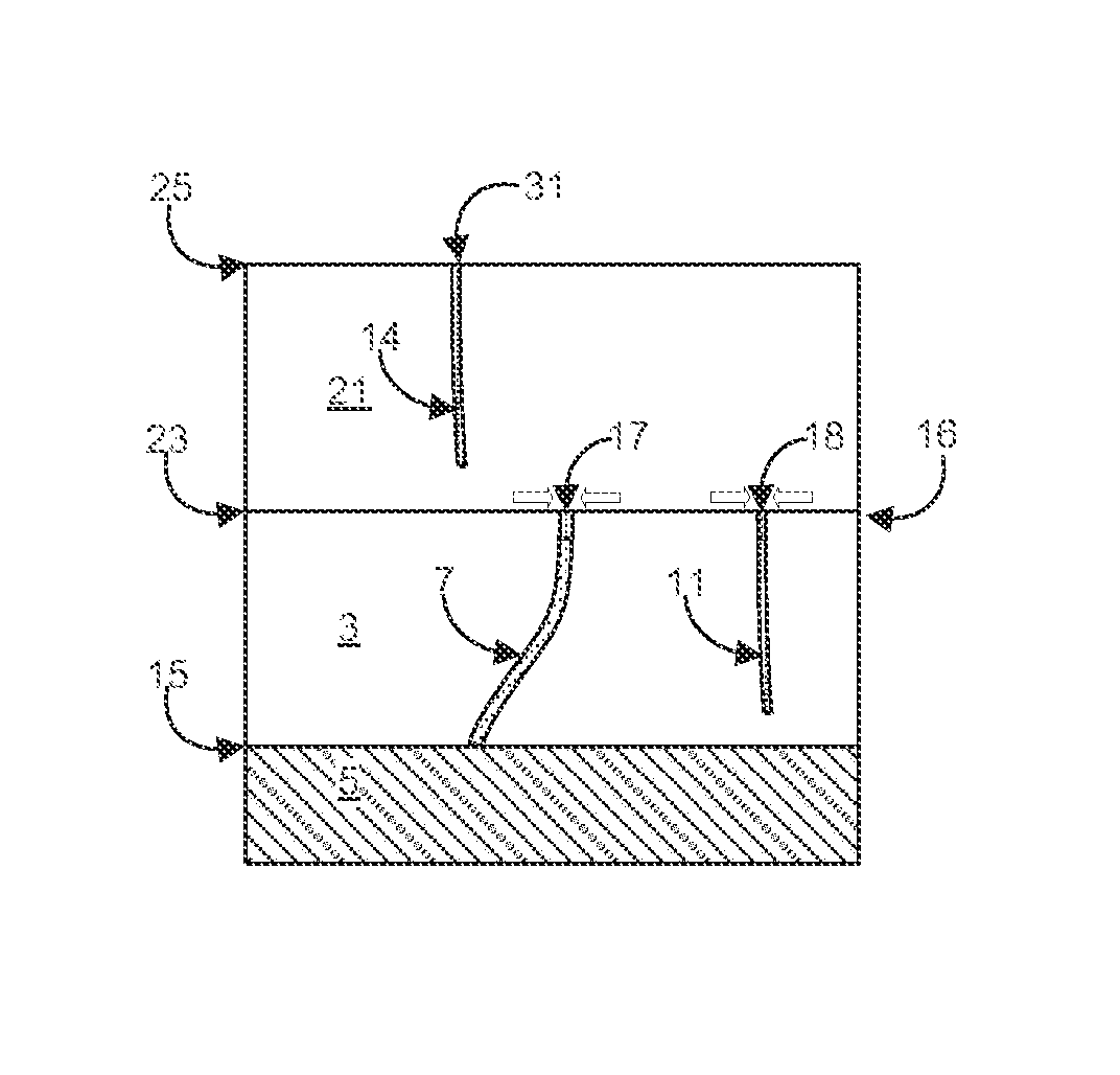
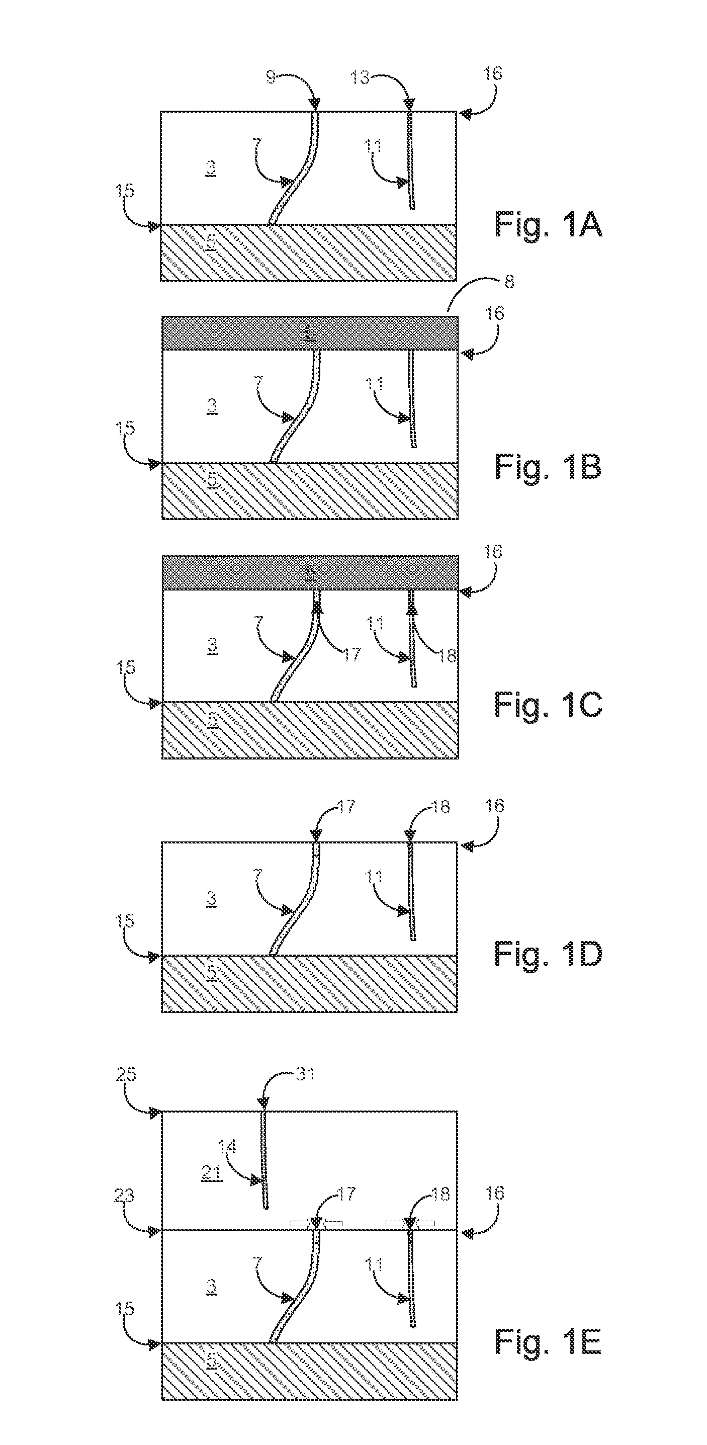
[0056]A (0001) sapphire substrate is utilized for the growth of gallium nitride layer 3. The substrate can be prepared for gallium nitride growth by preprocessing steps such as a cleaning cycle to remove unwanted contaminants (e.g. a high temperature bake in hydrogen containing ambient), a nitridization of the upper surface of the substrate, and further surface pretreatments dependent on the growth material and substrate.

[0057]Next a nucleation layer is deposited on the substrate and gallium nitride layer 3 is grown in a metalorganic chemical vapor deposition (MOCVD) reactor utilizing trimethlygallium (TMG) and ammonia (NH3) as precursor gases. First, the nucleation layer is deposited then thermally treated. Nucleation layer deposition is performed for a period of about 20 min by flowing TMG and NH3 while maintaining the reactor temperature at approximately 500° C. and the pressure at about 300 mb. Next, the nucleation layer is thermally treated by maintaining the reactor pressure a...

example 2

[0063]Many aspects of this example are similar to those of Example 1, and reference is made to that example for their description. Only aspects distinct from the previous example will be described.

[0064]The initial Group III-nitride layer (structure of FIG. 1A) with surface defects is grown as in Example 1. This structure is not removed from the deposition reactor utilized for deposition.

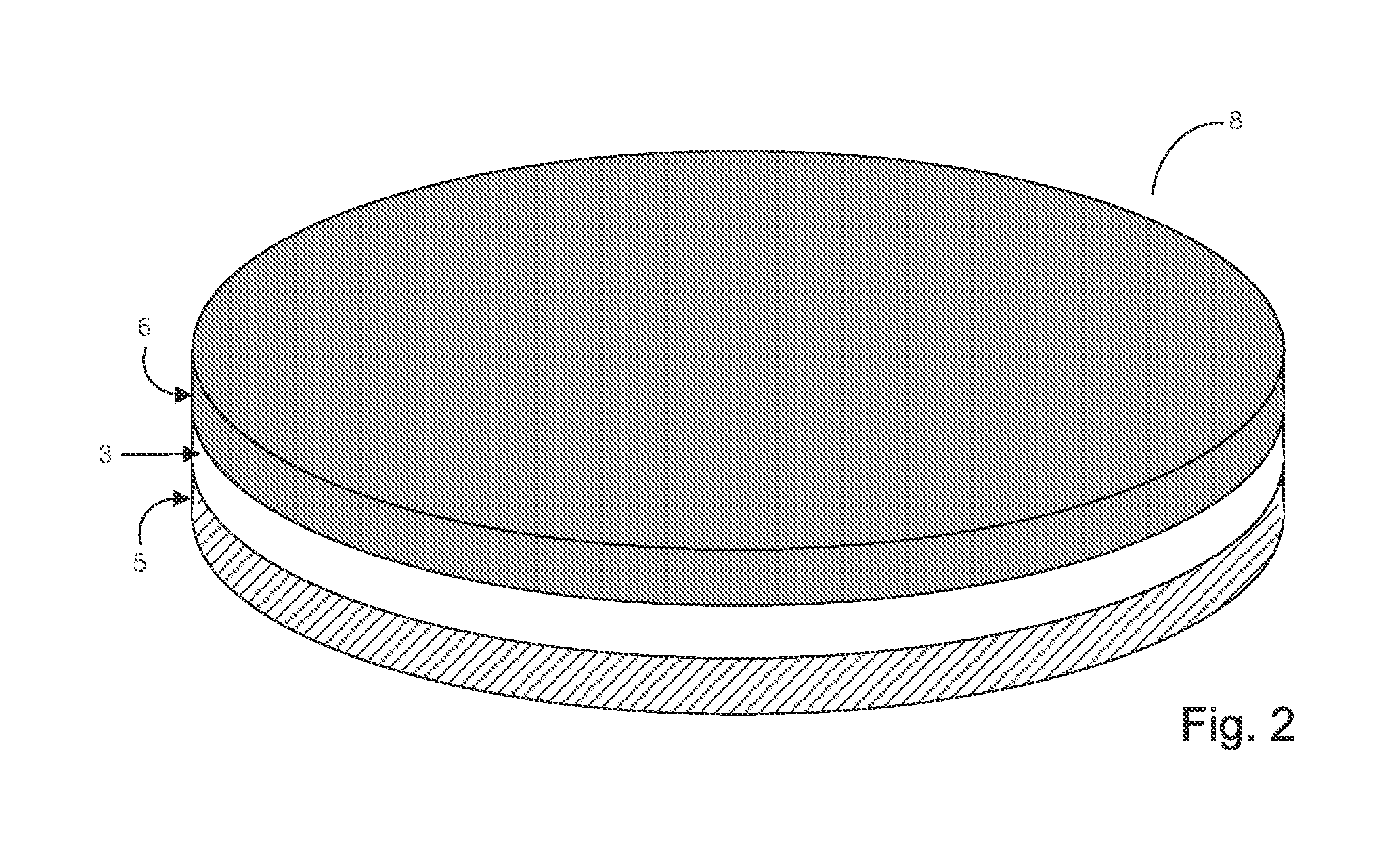
[0065]The temperature of the deposition reactor is then cooled from gallium nitride growth temperature (e.g. about 1100° C.) down to a temperature of approximately 600° C. over a time period of approximately 15 minutes. A protective layer comprising silicon nitride is now grown by introducing silane gas (or alternatively diethylsilane) and ammonia gas (or alternatively hydrazine, or a nitrogen gas vapor generated from a nitrogen based organometallic precursor) the deposition chamber for a growth time period of about 30 minutes and at a growth temperature of approximately 600° C. The thickness of the...


PUM

PropertyMeasurementUnit
temperatureaaaaaaaaaa

Abstract

The invention provides methods which can be applied during the epitaxial growth of two or more layers of Group III-nitride semiconductor materials so that the qualities of successive layer are successively improved. In preferred embodiments, surface defects interact with a protective layer of a protective material to form amorphous complex regions capable of preventing the further propagation of defects and dislocations. The invention also includes semiconductor structures fabricated by these methods.

Description

[0001]This application is a 371 filing of International Patent Application PCT / US2008 / 083630 filed Nov. 14, 2008, which claims the benefit of U.S. application No. 61 / 127,721 filed May 14, 2008.BACKGROUND[0002]1. Field of the Invention[0003]The invention relates to methods and structures utilized in the fabrication of high quality Group III-nitride materials. Embodiments of the invention are related to methods for improving the surface quality of Group III-nitride semiconductor material. In addition the invention also encompasses structures fabricated utilizing the methods of the invention.[0004]2. Background of the Invention[0005]The quality of a semiconductor material can considerably impact the performance of a solid state device produced from said material. Solid state devices can suffer from inferior lifetimes and operating characteristics when the semiconductor material encompasses an undesirable density of crystal defects, for example dislocations. Monocrystalline semiconducto...

Claims


Application Information

Patent Timeline
Patent Type & Authority Patents(United States)
IPC IPC(8): H01L21/469
CPCH01L21/0242H01L21/02458H01L21/0254H01L21/02639H01L21/02647
Inventor ARENA, CHANTALMAHAJAN, SUBHASH
Owner SOITEC SA
Why Eureka
Try Eureka