
Eureka
For R&D, Eureka makes reading and utilizing patents & technical documents easy.
Eureka AIR
Designed for self-driven R&D workflows. Generate viable solutions, solve complex R&D challenges, empower your innovation with AI.

Eureka Materials
Designed for material experts only. Revolutionize your material R&D, from search, analyze, to developing new materials.

TechResearch
Generate reliable direction feasibility study reports for your R&D in just a few steps.

TechSeek
Discover and master advanced knowledge NOW. Basics, ideas, possibilities, all at once.

TechMind
As an expert in R&D Theories, TechMind can generates customized viable solutions instantly.

TechRisk
Analyze your overall solution with one click, know your potential R&D risks in advance.

TechMonitor
Get weekly tech updates, stay abreast of the latest tech innovations and key insights.
Nonvolatile semiconductor memory device
- Summary
- Abstract
- Description
- Claims
- Application Information
AI Technical Summary
Benefits of technology
Problems solved by technology
Method used
Image

Examples
first example
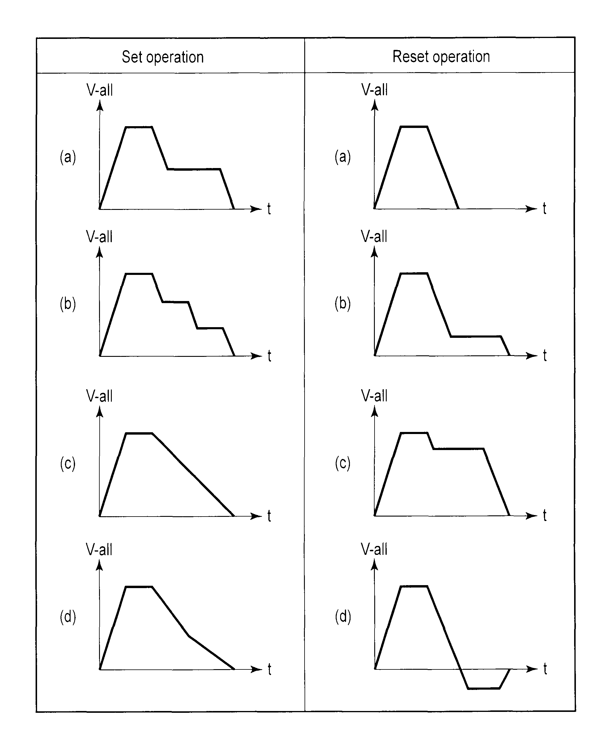
[0111]With reference to FIG. 11, a first example of set / reset operations is described. The first example may be applied to, for example, a bipolar-type variable resistance element.
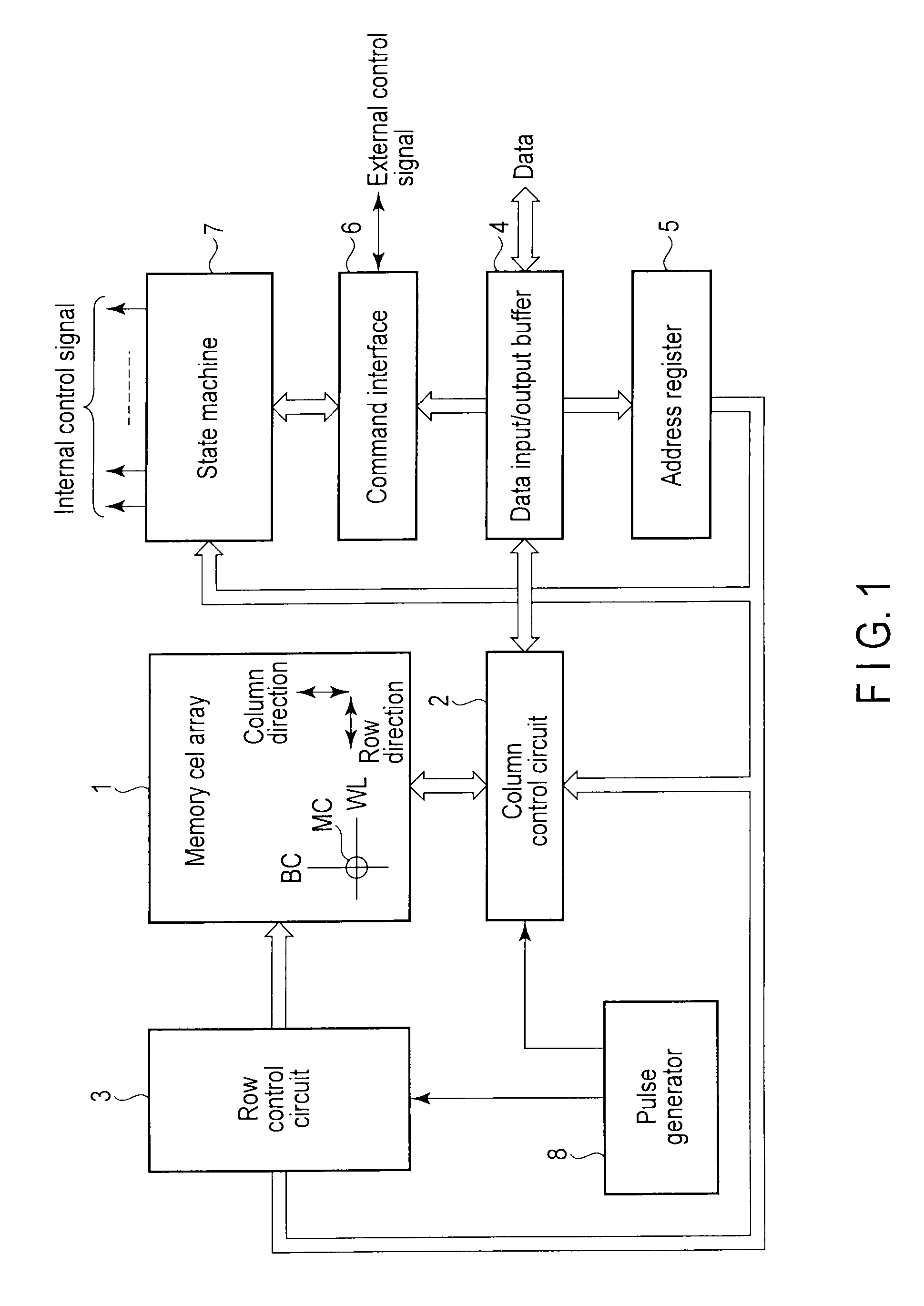
[0112]As illustrated in FIG. 12, in a data-writing (set) operation, column control circuit 2 applies voltage V1 to selected bit line BL1, and applies voltage V2 to each of unselected bit lines BL0, BL2, and BL3. Moreover, row control circuit 3 applies 0 V to selected word line WL1, and applies voltage V2 to each of unselected word lines WL0, WL2, and WL3.
[0113]In short, the relationship between the voltages (V1 and V2) is changed from state 1 in FIG. 11 to state 2 therein.
[0114]Voltages V1 and V2 are each a positive voltage, and voltage V1 is larger than voltage V2. For example, voltages V1 and V2 have a relationship of V1=2×V2.
[0115]In this way, entire voltage V-all applied to selected memory cell MC-sel is set to voltage V1. Thus, variable resistance element VR that is of an electric field depending type...
second example
[0148]With reference to FIG. 17, a description is made about a second example of the set / reset operations in the embodiment. The second example may be applied to, for example, a monopolar-type variable resistance element.
[0149]As illustrated in FIG. 12, in a data-writing (set) operation, column control circuit 2 first applies voltage V1 to selected bit line BL1, and applies voltage V2 to each of unselected bit lines BL0, BL2, and BL3. Moreover, row control circuit 3 applies 0 V to selected word line WL1, and applies voltage V2 to each of unselected word lines WL0, WL2, and WL3.
[0150]In short, the relationship between the voltages of the lines is changed from state 1 in FIG. 11 to state 2 therein.
[0151]In the same manner as in the first example, the entire voltage V-all applied to selected memory cell MC-sel is set to voltage V1, whereby variable resistance element VR therein is changed from a high resistance state to a low resistance state. However, voltage V1 needs to be equal to o...
third example
[0176]With reference FIG. 19, a description is made about a third example of the set / reset operations in the embodiment. The third example is a modified example of the first example.
[0177]Any data writing (set) operation is the same as in the first example; thus, a detailed description thereon is omitted herein. The third example is characterized by data erasing (reset) operation.
[0178]As illustrated in FIG. 12, in the reset operation, column control circuit 2 first applies voltage V1 to selected bit line BL1, and applies voltage V2 to each of unselected bit lines BL0, BL2, and BL3. Moreover, row control circuit 3 applies 0 V to selected word line WL1, and applies voltage V2 to each of unselected bit lines WL0, WL2, and WL3.
[0179]In short, the relationship between the voltages of the lines is changed from state 1 in FIG. 19 to state 2 therein.
[0180]Thereafter, state 3 in FIG. 19 is skipped, and state 2 is immediately changed to state 4.
[0181]Specifically, as illustrated in, for, exa...
PUM
 Abstract
Description
Claims
Application Information
 - R&D Engineer
- R&D Manager
- IP Professional
- Industry Leading Data Capabilities
- Powerful AI technology
- Patent DNA Extraction
Browse by: Latest US Patents, China's latest patents, Technical Efficacy Thesaurus, Application Domain, Technology Topic, Popular Technical Reports.
© 2024 PatSnap. All rights reserved.Legal|Privacy policy|Modern Slavery Act Transparency Statement|Sitemap|About US| Contact US: help@patsnap.com