Low power optical interconnect driver circuit

a driver circuit and low power technology, applied in static indicating devices, instruments, electroluminescent light sources, etc., can solve the problems of increasing the cost of the system even more, increasing the cost of the system, and prohibiting traditional optical data links, so as to reduce the power dissipation and reduce the load burden on the driving input signal, the effect of low capacitance values

Active Publication Date: 2013-02-12
WAVEFRONT RES
View PDF32 Cites 2 Cited by
  • Summary
  • Abstract
  • Description
  • Claims
  • Application Information

AI Technical Summary

Benefits of technology

[0019]In one embodiment of the circuit of this invention, the light emitting semiconductor device is driven from a completely OFF condition (no bias used), through the non-linear region of operation to a point above the lasing threshold, but still providing a predictable photonic output. During circuit operation the only power dissipated is during the interval when the capacitor charges or discharges; there is substantially no DC current component (except for leakage currents and the like). The current through the light emitting semiconductor device is both time dependent and intermittent. The charging or discharging is a dynamic one-time event, regardless of the resting state of the input logic signal. Moreover, in many embodiments substantially low capacitance values can be used, which results in a low load burden on the driving input signal.
[0020]The driver circuit of the present invention can reduce the power dissipation substantially by using a pulsed driver scheme that passively reduces the duty cycle of the data stream.
[0021]In embodiments of the driver circuit of this invention, a light emitting semiconductor device (a VCSEL in one embodiment) can be modulated ON / OFF in a controlled, pulsed duty cycle without the burden of the extra power requirement normally associated with the circuit elements controlling pulse width and bias requirements. This can allow for a comparatively low, overall power dissipation in an optical interconnect system.

Problems solved by technology

In optical interconnect systems, when the interconnect channel density becomes many hundreds of interconnects and even greater per square inch, the thermal gradients and thermal dissipation in the interconnect elements themselves become a major issue.
This undesirable trait costs the system even more energy to extract this thermal load from the interconnect component area, particularly when active cooling devices such as thermo-electric (Peltier) coolers are required.
In a Dewar environment, traditional optical data links become prohibitive due to the undesired thermal load contributions to the cold side of the Dewar system.

Method used


Image

  • Low power optical interconnect driver circuit
  • Low power optical interconnect driver circuit
  • Low power optical interconnect driver circuit

Examples


embodiment 10

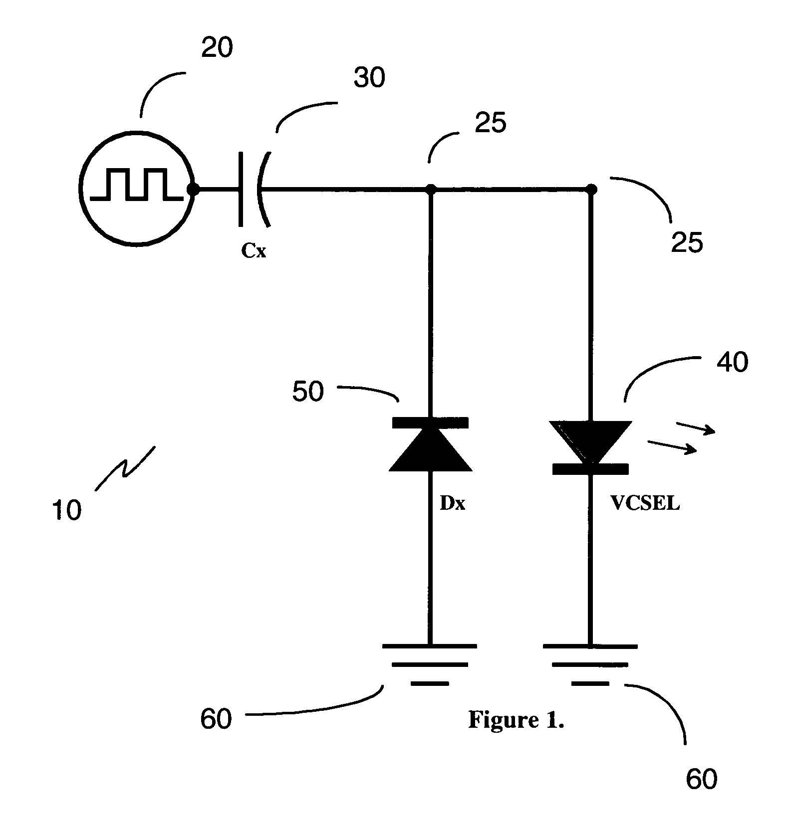
[0032]An embodiment 10 of the driver circuit of this invention for driving a light emitting semiconductor device (a VCSEL in the embodiment shown) is shown in FIG. 1.

[0033]Referring to FIG. 1, the embodiment 10 of the driver circuit of this invention includes a capacitor 30 connected between a source of voltage pulses 20 and a terminal 25 of the light emitting semiconductor device 40 (a VCSEL 40 in the embodiment shown), the light emitting semiconductor device 40 being connected so that a forward current flow direction of the light emitting semiconductor device (indicated by the pointed portion of the symbol used to represent the light emitting semiconductor device 40) is away from the terminal 25, and, a diode 50 connected in parallel to the light emitting semiconductor device 40. The diode 50 is connected so that a direction of forward current flow of the diode 50 is opposite to the forward current flow direction of the light emitting semiconductor device 40. In the embodiment sho...

embodiment 100

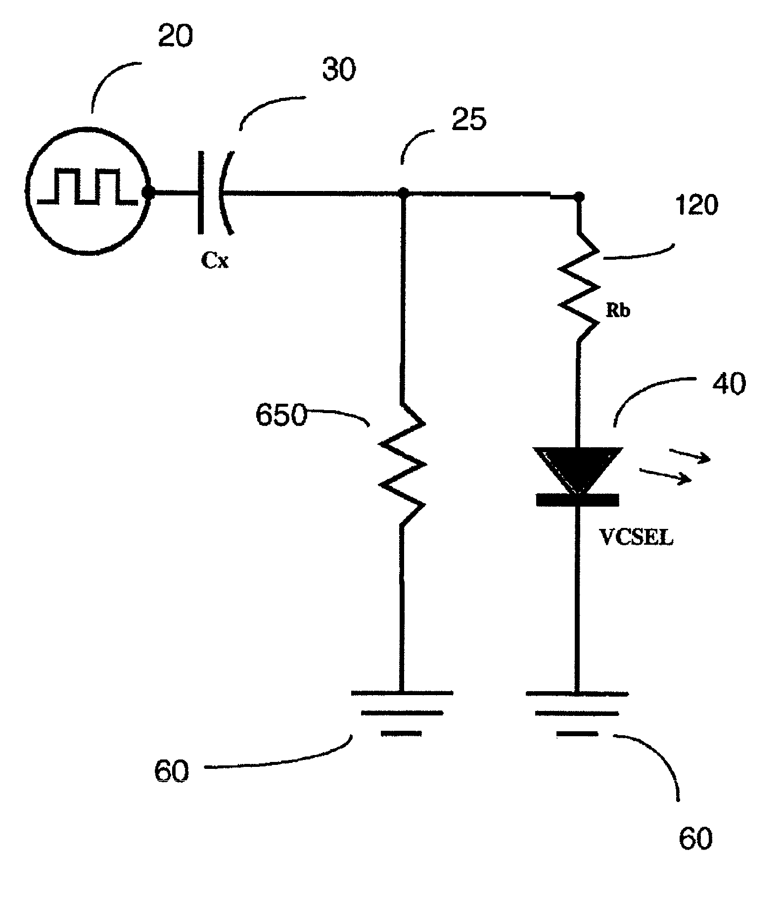
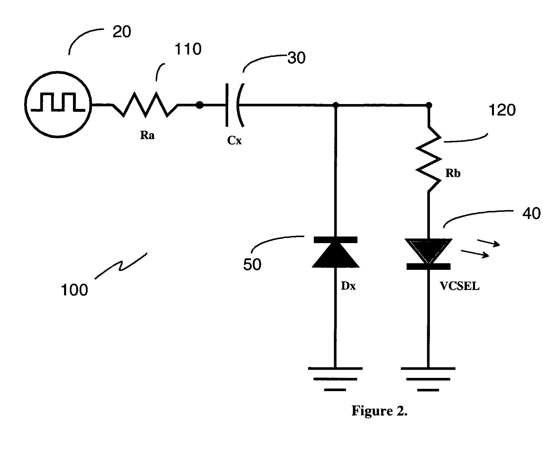
[0036]The embodiment 100 of the driver circuit of this invention, shown in FIG. 2, includes a resistor 110 connected in series with the capacitor 30 (Cx) and / or another resistor 120 connected in series with the light emitting semiconductor device 40, the diode 50 being connected in parallel with the series combination of other resistor 120 and the light emitting semiconductor device 40. Circuit functionality is unchanged but this embodiment can allow for additional tailoring of duration and magnitude of the pulse currents. In certain applications it may be desirable to tailor capacitor charge rates to allow a greater range of capacitor values and limit current / voltage rise rates (thereby altering the pulse shape of the optical emission).

embodiment 200

[0037]The embodiment 200 of the driver circuit of this invention shown in FIG. 3 includes two light emitting semiconductor devices 210, 220 (VCSEL devices in the embodiment shown) wired in parallel and having opposite polarities (also referred to as one light emitting semiconductor device 210 and the other light emitting semiconductor device 220 are located, positioned or oriented such that a direction of forward current flow of the one light emitting semiconductor device 210 is opposite to the forward current flow direction of the other light emitting semiconductor device 220) allowing one semiconductor device to emit radiation at the rising edge of the input signal and the other to emit radiation at the falling edge of the input signal. The capacitor 30 charges through one light emitting semiconductor device (VCSEL) 210 and discharges through the second light emitting semiconductor device (VCSEL) 220. In this embodiment, the second light emitting semiconductor device (VCSEL) 220 r...


PUM


Abstract

A driver circuit for driving a light emitting semiconductor device. The driver circuit of this invention includes a capacitor connected between a source of voltage pulses and a light emitting semiconductor device.

Description

CROSS REFERENCE TO RELATED APPLICATIONS[0001]This application claims priority of U.S. Provisional Application 60 / 491,496 filed on Jul. 31, 2003, which is incorporated by reference herein.STATEMENT OF GOVERNMENT INTEREST[0002]This invention was partially made with U.S. Government support from the U.S. Navy under contracts #N00178-03-C-1024 and #N00178-04-C-1034. The U.S. Government has certain rights in the invention.BACKGROUND OF THE INVENTION[0003]This invention relates generally to optical interconnect driver circuits, and, more particularly to systems and methods for driving a light emitting semiconductor device.[0004]In optical interconnect systems, when the interconnect channel density becomes many hundreds of interconnects and even greater per square inch, the thermal gradients and thermal dissipation in the interconnect elements themselves become a major issue. This undesirable trait costs the system even more energy to extract this thermal load from the interconnect componen...

Claims


Application Information

Patent Timeline
Patent Type & Authority Patents(United States)
IPC IPC(8): G09G3/32
CPCH05B33/0821H02M7/06H05B45/42
Inventor VEITCH, RANDALL C.
Owner WAVEFRONT RES
Why Eureka
Try Eureka