Current mirror semiconductor device and a layout method of the same

a current mirror semiconductor and layout method technology, applied in the direction of electric variable regulation, process and machine control, instruments, etc., can solve the problems of affecting the performance of transistors, affecting the efficiency of semiconductor devices, so as to reduce the number of mismatch errors

Active Publication Date: 2013-03-19
SK HYNIX INC
View PDF12 Cites 0 Cited by
  • Summary
  • Abstract
  • Description
  • Claims
  • Application Information

AI Technical Summary

Benefits of technology

[0023]The present invention provides a current mirror semiconductor device having a mirror structure electronic configuration and a layout method of the same, which can reduce a mismatch error associated with transistors built with a combination of masks.
[0024]The present invention can provide an advantage of reduces offset of transistors to improve mass productivity and reliability of a semiconductor device.

Problems solved by technology

These differences often occur due to mismatching of the various combinations of masks, etc.
A mismatch in the combination of the masks leads to mismatch errors in transistors that often times result in performance degradation of the transistors.
These types of semiconductor devices seem to be more prone to being adversely affected by mismatching a combination of the masks.
As a result of this symmetrically laid out design, the resultant transistors suffer a large number of mismatch errors as a result of the mismatch alignment of the plurality of transistors employing these combinations of masks.
Therefore, the performance of semiconductor devices, in particular current mirror configurations, can be adversely affected by mismatch errors when combining the masks to build symmetrically laid out devices.
Also, even though the NMOS transistor N1 is connected at a point which is substantially at an exact halfway point from the sources of the NMOS transistors N0, N0B; these mismatch errors can still adversely affect the resultant NMOS transistor N0 having the same arrangement structure and the NMOS transistor N0B having the opposite arrangement structure.

Method used


Image

  • Current mirror semiconductor device and a layout method of the same
  • Current mirror semiconductor device and a layout method of the same
  • Current mirror semiconductor device and a layout method of the same

Examples


first embodiment

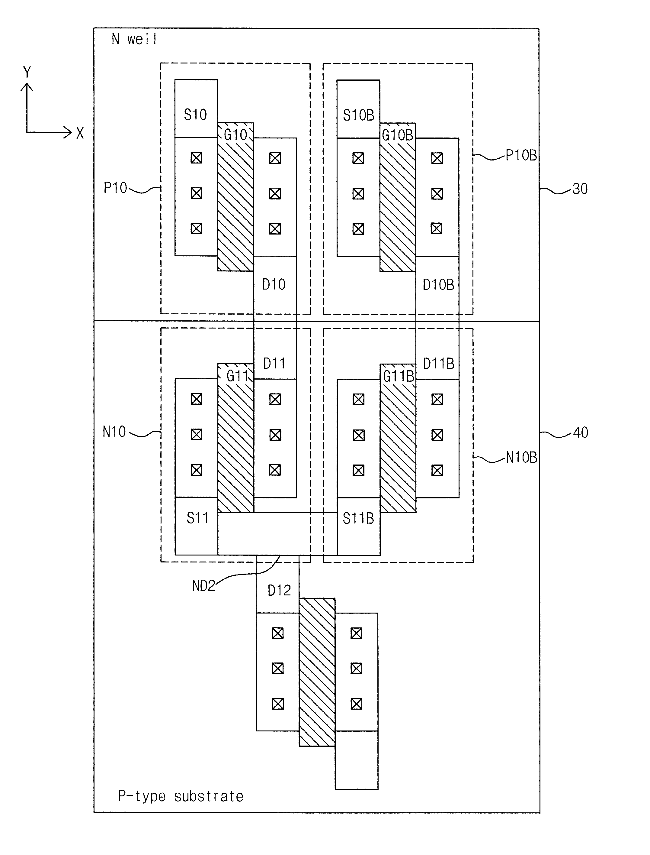
[0054]The present invention discloses a voltage generator as a semiconductor device having a current mirror electronic configuration structure.

[0055]As depicted in FIG. 4, the voltage generator includes PMOS transistors P10, P10B, P11 and NMOS transistors N10, N10B, N11.

[0056]Specifically, sources of the PMOS transistors P10, P10B are shown connected to a power supply voltage terminal VDD; drains of the NMOS transistors N10, N10B are shown connected to drains of PMOS transistor P10, P10B; and a drain of the NMOS transistor N11 is shown connected to a node ND2 to which the sources of the NMOS transistors N10, N10B are shown commonly connected and a source thereof is shown to be connected to a ground voltage terminal VSS.

[0057]The gates of the PMOS transistors P10, P10B are shown connected to a common drain of the PMOS transistor P10B and the NMOS transistor N10B and respective gates of the NMOS transistors N10, N10B are shown to be applied with a reference voltage VREFC and a compari...

second embodiment

[0075]the present invention will be described by a reference voltage generator.

[0076]Generally, the reference voltage generator is a device which generates reference potential insensitive to changes in process, voltage, and temperature. As a representative type of the reference voltage generator, there are a Widlar type and a Bandgap type.

[0077]Referring to FIG. 8, the Widlar type of the reference voltage generator includes PMOS transistors P20, P20B, NMOS transistors N20, N20B, and a resistor R1.

[0078]Specifically, sources of the PMOS transistors P20, P20B are shown connected to a power supply voltage terminal VDD, drains of the NMOS transistors N20, N20B are shown connected drains of each PMOS transistors P20, P20B, a source of the NMOS transistor N20 is shown connected to one terminal of the resistor R1, a source of the NMOS transistor N20B is shown connected to a ground voltage terminal VSS, and the other terminal of the resistor R1 is shown connected to a ground voltage termina...

third embodiment

[0093]the present invention will be described by a data sense amplifier.

[0094]Referring to FIG. 12, the data sense amplifier, which compares and amplifies a voltage difference between input / output lines LIO, LIOB transferring data amplified in a bit line sense amp and outputs it to global input / output lines G10, G10B, includes PMOS transistors P50, P50B and NMOS transistors N50, N50B, N51, N51B, N52.

[0095]Specifically, sources of the PMOS transistors P50, P50B are shown connected to a power supply voltage terminal VDD, drains of the NMOS transistors N50, N50B are shown connected drains of each PMOS transistors P50, P50B, drains of the NMOS transistors N51, N51B are connected to sources of each NMOS transistors N50, N50B, and a drain of the NMOS transistor N52 is shown connected to a common source of the NMOS transistors N51, N51B, and a source thereof is shown connected to a ground voltage terminal VSS.

[0096]The gates of the PMOS transistor P50 and the NMOS transistor N50 and the gl...


PUM


Abstract

A semiconductor device and a layout method of the same reduce a mismatch in a semiconductor device. The semiconductor device includes a first transistor unit providing a first path of current and a second transistor unit designed in a mirror structure to the first transistor unit and providing a second path of current. The layout of the second transistor unit has a shape identical to the first transistor unit and shifted in a first direction. The layout of the semiconductor device reduces a mismatch of the transistors occurring when masks are combined, and thereby reduces their offset.

Description

CROSS-REFERENCE TO RELATED APPLICATIONS[0001]The present application claims priority to Korean patent application number 10-2007-0091692 filed on Sep. 10, 2007, which is incorporated herein by reference in its entirety.BACKGROUND OF THE INVENTION[0002]The present invention relates to semiconductor devices and to layout methods, and more particularly to a current mirror semiconductor device and a layout method of the same, which can reduce mismatching layout errors of a semiconductor device having a mirror structure.[0003]Typically, semiconductor devices are formed with transistors made by a combination of different masks. These masks are manufactured to produce several tens of layers and are combined, and patterns of the masks are formed using a photo device. Dies within a wafer are designed under the same or similar conditions, but slight differences in positions within the wafer may occur due to various variables during processing. These differences often occur due to mismatching ...

Claims


Application Information

Patent Timeline
Patent Type & Authority Patents(United States)
IPC IPC(8): G05F3/16
CPCG05F3/267G06F17/5068G06F30/39H01L27/04
Inventor LEE, KANG SEOL
Owner SK HYNIX INC
Why Eureka
Try Eureka