Advanced transistors with punch through suppression

a transistor and punch-through technology, applied in the direction of transistors, semiconductor devices, electrical equipment, etc., can solve the problems of difficult to achieve, adversely affect the electron mobility, and inability to achieve simple proportional shrinkag

Active Publication Date: 2013-04-16
MIE FUJITSU SEMICON
View PDF514 Cites 30 Cited by
  • Summary
  • Abstract
  • Description
  • Claims
  • Application Information

AI Technical Summary

Benefits of technology

[0003]Fitting more transistors onto a single die is desirable to reduce cost of electronics and improve their functional capability. A common strategy employed by semiconductor manufacturers is to simply reduce gate size of a field effect transistor (FET), and proportionally shrink area of the transistor source, drain, and required interconnects between transistors. However, a simple proportional shrink is not always possible because of what are known as “short channel effects”. Short channel effects are particularly acute when channel length under a transistor gate is comparable in magnitude to depletion depth of an operating transistor, and include reduction in threshold voltage, severe surface scattering, drain induced barrier lowering (DIBL), source-drain punch through, and electron mobility issues.

Problems solved by technology

However, a simple proportional shrink is not always possible because of what are known as “short channel effects”.
Unfortunately, while such implants improve some electrical characteristics such as threshold voltage rolloff and drain induced barrier lowering, the resultant increased channel doping adversely affects electron mobility, primarily because of the increased dopant scattering in the channel.
Unfortunately, creating a suitable insulator layer is expensive and difficult to accomplish.
Early SOI devices were built on insulative sapphire wafers instead of silicon wafers, and are typically only used in specialty applications (e.g. military avionics or satellite) because of the high costs.
Modern SOI technology can use silicon wafers, but require require expensive and time consuming additional wafer processing steps to make an insulative silicon oxide layer that extends across the entire wafer below a surface layer of device-quality single-crystal silicon.
As would be expected, both BOX formation or layer transfer are costly manufacturing techniques with a relatively high failure rate.
Accordingly, manufacture of SOI transistors not an economically attractive solution for many leading manufacturers.
Considering the likely need for complex non-planar transistor manufacturing techniques to make a finFET, and the unknown difficulty in creating a new process flow for finFET, manufacturers have been reluctant to invest in semiconductor fabrication facilities capable of making finFETs.

Method used


Image

  • Advanced transistors with punch through suppression
  • Advanced transistors with punch through suppression
  • Advanced transistors with punch through suppression

Examples


Embodiment Construction

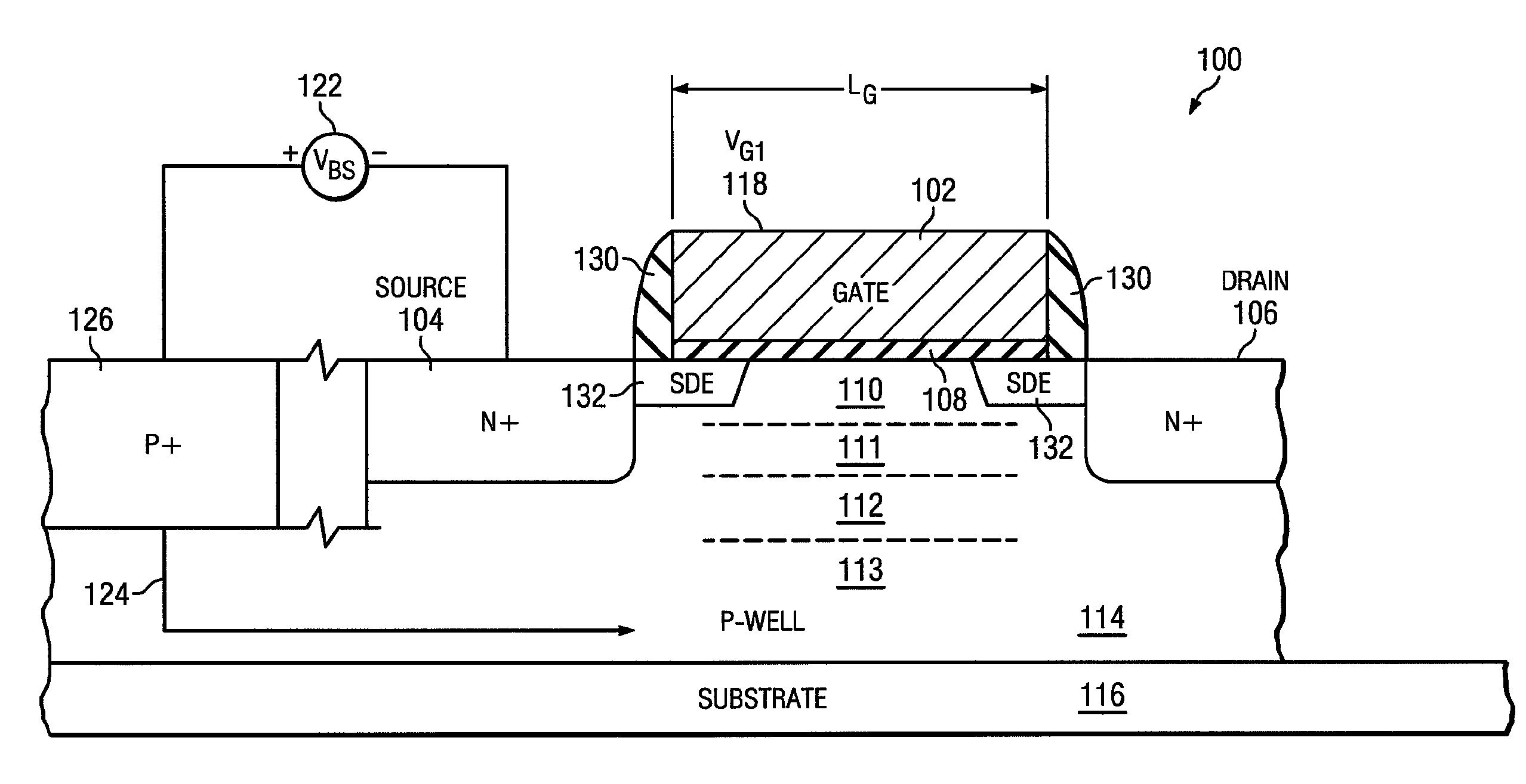
[0013]Unlike silicon on insulator (SOI) transistors, nanoscale bulk CMOS transistors (those typically having a gate length less than 100 nanometers) are subject to significant adverse short channel effects, including body leakage through both drain induced barrier lowering (DIBL) and source drain punch through. Punch through is associated with the merging of source and drain depletion layers, causing the drain depletion layer to extend across a doped substrate and reach the source depletion layer, creating a conduction path or leakage current between the source and drain. This results in a substantial increase in required transistor electrical power, along with a consequent increase in transistor heat output and decrease in operational lifetime for portable or battery powered devices using such transistors.

[0014]An improved transistor manufacturable on bulk CMOS substrates is seen in FIG. 1. A Field Effect Transistor (FET) 100 is configured to have greatly reduced short channel effe...


PUM


Abstract

An advanced transistor with punch through suppression includes a gate with length Lg, a well doped to have a first concentration of a dopant, and a screening region positioned under the gate and having a second concentration of dopant. The second concentration of dopant may be greater than 5×10¹⁸ dopant atoms per cm3. At least one punch through suppression region is disposed under the gate between the screening region and the well. The punch through suppression region has a third concentration of a dopant intermediate between the first concentration and the second concentration of dopant. A bias voltage may be applied to the well region to adjust a threshold voltage of the transistor.

Description

RELATED APPLICATIONS[0001]This application claims the benefit of U.S. Provisional Application No. 61 / 247,300, filed Sep. 30, 2009, the disclosure of which is incorporated by reference herein. This application also claims the benefit of U.S. Provisional Application No. 61 / 262,122, filed Nov. 17, 2009, the disclosure of which is incorporated by reference herein, and U.S. patent application Ser. No. 12 / 708,497, titled “Electronic Devices and Systems, and Methods for Making and Using the Same”, filed Feb. 18, 2010, the disclosure of which is incorporated by reference herein. This application also claims the benefit of U.S. Provisional Application No. 61 / 357,492, filed Jun. 22, 2010, the disclosure of which is incorporated by reference herein.FIELD OF THE INVENTION[0002]This disclosure relates to structures and processes for forming advanced transistors with improved operational characteristics, including enhanced punch through suppression.BACKGROUND OF THE INVENTION[0003]Fitting more tr...

Claims


Application Information

Patent Timeline
Patent Type & Authority Patents(United States)
IPC IPC(8): H01L29/772H01L21/336
CPCH01L21/823412H01L21/82345H01L21/823493H01L27/088H01L29/1083H01L29/7833H01L29/7836H01L29/78H01L29/1045H01L29/7816H01L29/66537H01L27/092H01L29/0847H01L29/1033H01L29/36
Inventor SHIFREN, LUCIANRANADE, PUSHKARGREGORY, PAUL E.SONKUSALE, SACHIN R.ZHANG, WEIMINTHOMPSON, SCOTT E.
Owner MIE FUJITSU SEMICON
Why Eureka
Try Eureka