Non-volatile memory and method with even/odd combined block decoding

a technology of combined block decoding and non-volatile memory, which is applied in the field of non-volatile semiconductor memory, can solve the problems of large size and net gain in space saving, and achieve the effects of saving space, space saving, and halving the number of decoding circuits

Active Publication Date: 2013-04-23
SANDISK TECH LLC
View PDF19 Cites 8 Cited by
  • Summary
  • Abstract
  • Description
  • Claims
  • Application Information

AI Technical Summary

Benefits of technology

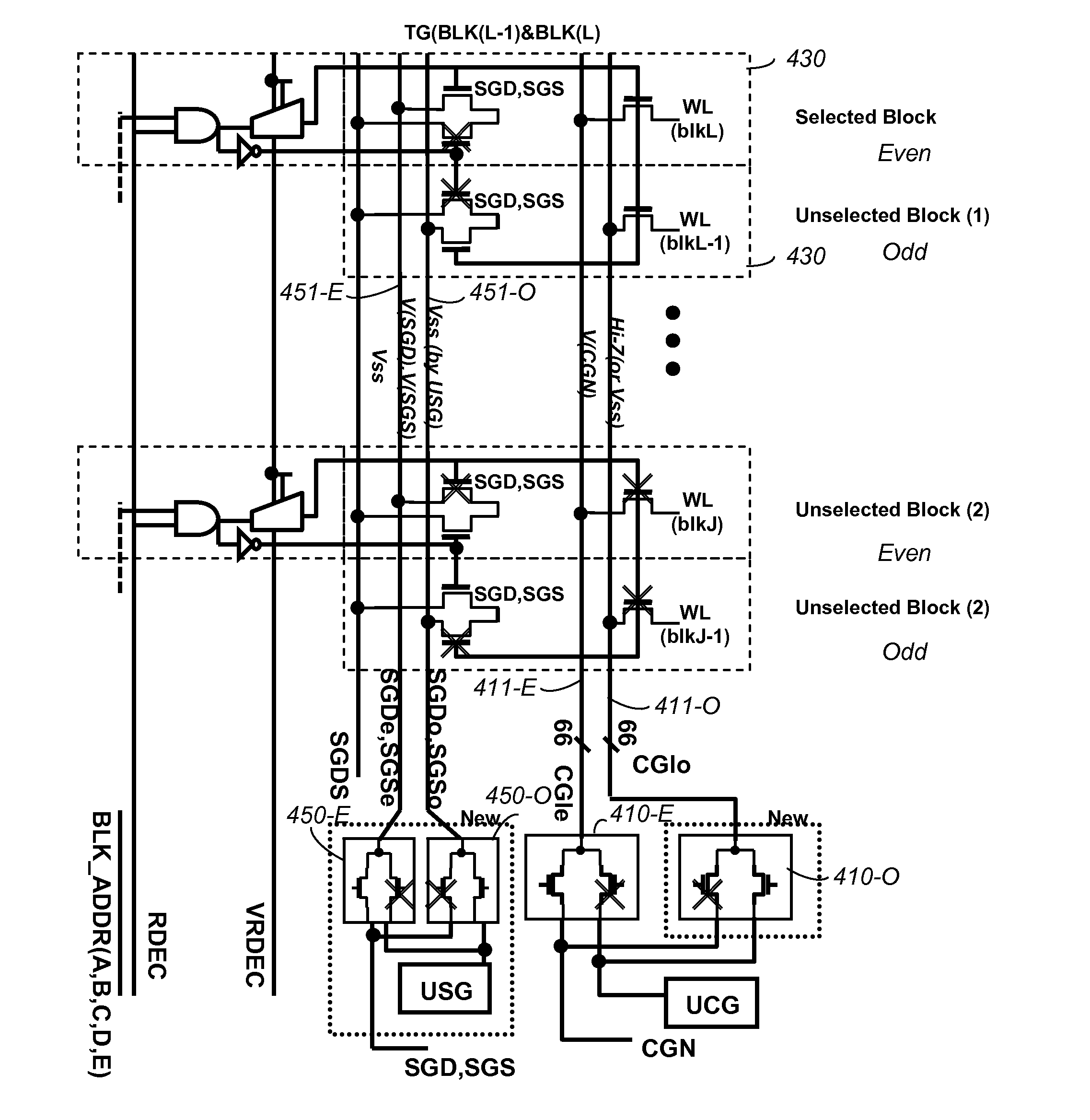
[0015]The row or block decoders are implemented in circuit elements able to withstand the high voltages needed by the word lines. Consequently, they are necessarily of relatively large size. By decoding two blocks at a time, the number of decoding circuits is halved and space saving can be realized, although at the expense of doubling the number voltage buses. However, there is a net gain in saving space because the saving is gained with increasing number of blocks while the expense remains the same. Also, the doubling of the voltage buses will reduce by a half the junction capacitance on the word lines.

Problems solved by technology

Consequently, they are necessarily of relatively large size.
However, there is a net gain in saving space because the saving is gained with increasing number of blocks while the expense remains the same.

Method used


Image

  • Non-volatile memory and method with even/odd combined block decoding
  • Non-volatile memory and method with even/odd combined block decoding
  • Non-volatile memory and method with even/odd combined block decoding

Examples


Embodiment Construction

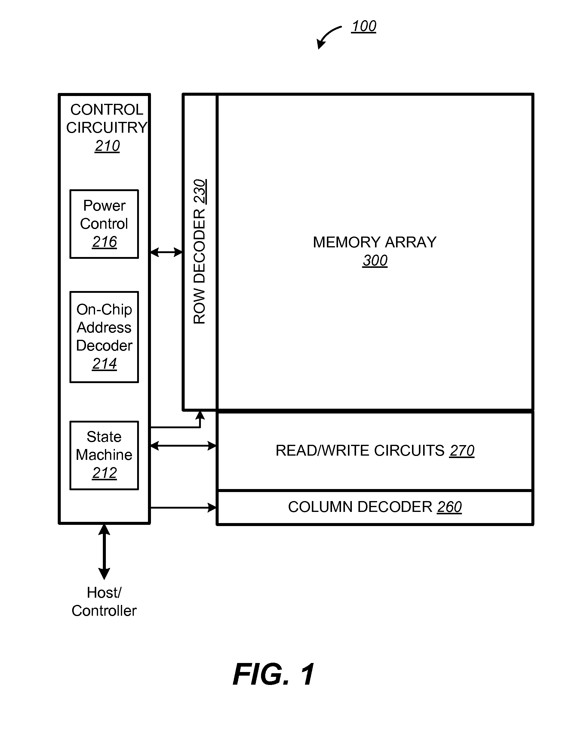
[0030]FIG. 1 illustrates schematically a compact memory device which provides the context in which the present invention is implemented. The memory device 100, usually in the form of a memory chip, includes a two-dimensional array of memory cells 300, control circuitry 210, and read / write circuits 270. The memory array 300 is addressable by word lines via a row decoder 230 and by bit lines via a column decoder 260. The read / write circuits 270 allow a page of memory cells to be read or programmed in parallel.

[0031]The control circuitry 210 cooperates with the read / write circuits 270 to perform memory operations on the memory array 300. It also interfaces with an external host or a memory controller to exchange. The control circuitry 210 includes a state machine 212, an on-chip address decoder 214 and a power control module 216. The state machine 212 provides chip level control of memory operations. The on-chip address decoder 214 provides an address interface between that used by the...


PUM


Abstract

A nonvolatile memory array is organized into a plurality of interleaving even and odd blocks. When a block is selected for operation, a set of word line voltages are delivered to the block of word lines by space-efficient decoding circuits and scheme. The plurality of blocks is organized into an array of pairs of adjacent odd and even blocks. A first voltage bus allows all even blocks access to the set of word line voltages. A second voltage bus allows all odd blocks access to the set of word line voltages. A decoder for selection is provided for each pair of adjacent even and odd blocks. Selecting a block is effected by selecting the pair of adjacent even and odd blocks containing the selected block, and supplying the set of word line voltages only to the selected block, which is one of the even or odd block in the selected pair.

Description

CROSS-REFERENCE TO RELATED APPLICATION[0001]The benefit is claimed of U.S. provisional patent application of Yosuke Kato, Application No. 61 / 329,674 filed on Apr. 30, 2010.FIELD OF THE INVENTION[0002]This invention relates generally to non-volatile semiconductor memory such as electrically erasable programmable read-only memory (EEPROM) and flash EEPROM, and specifically to efficient implementation of row decoders for the memory array.BACKGROUND OF THE INVENTION[0003]Solid-state memory capable of nonvolatile storage of charge, particularly in the form of EEPROM and flash EEPROM packaged as a small form factor card, has recently become the storage of choice in a variety of mobile and handheld devices, notably information appliances and consumer electronics products. Unlike RAM (random access memory) that is also solid-state memory, flash memory is non-volatile, and retaining its stored data even after power is turned off. Also, unlike ROM (read only memory), flash memory is rewritabl...

Claims


Application Information

Patent Timeline
Patent Type & Authority Patents(United States)
IPC IPC(8): G11C16/04
CPCG11C8/04G11C16/08G11C16/0483G11C8/08G11C8/10
Inventor KATO, YOSUKE
Owner SANDISK TECH LLC
Why Eureka
Try Eureka