Non-volatile memory and method with even/odd combined block decoding
- Summary
- Abstract
- Description
- Claims
- Application Information
AI Technical Summary
Benefits of technology
Problems solved by technology
Method used
Image

Examples
Embodiment Construction
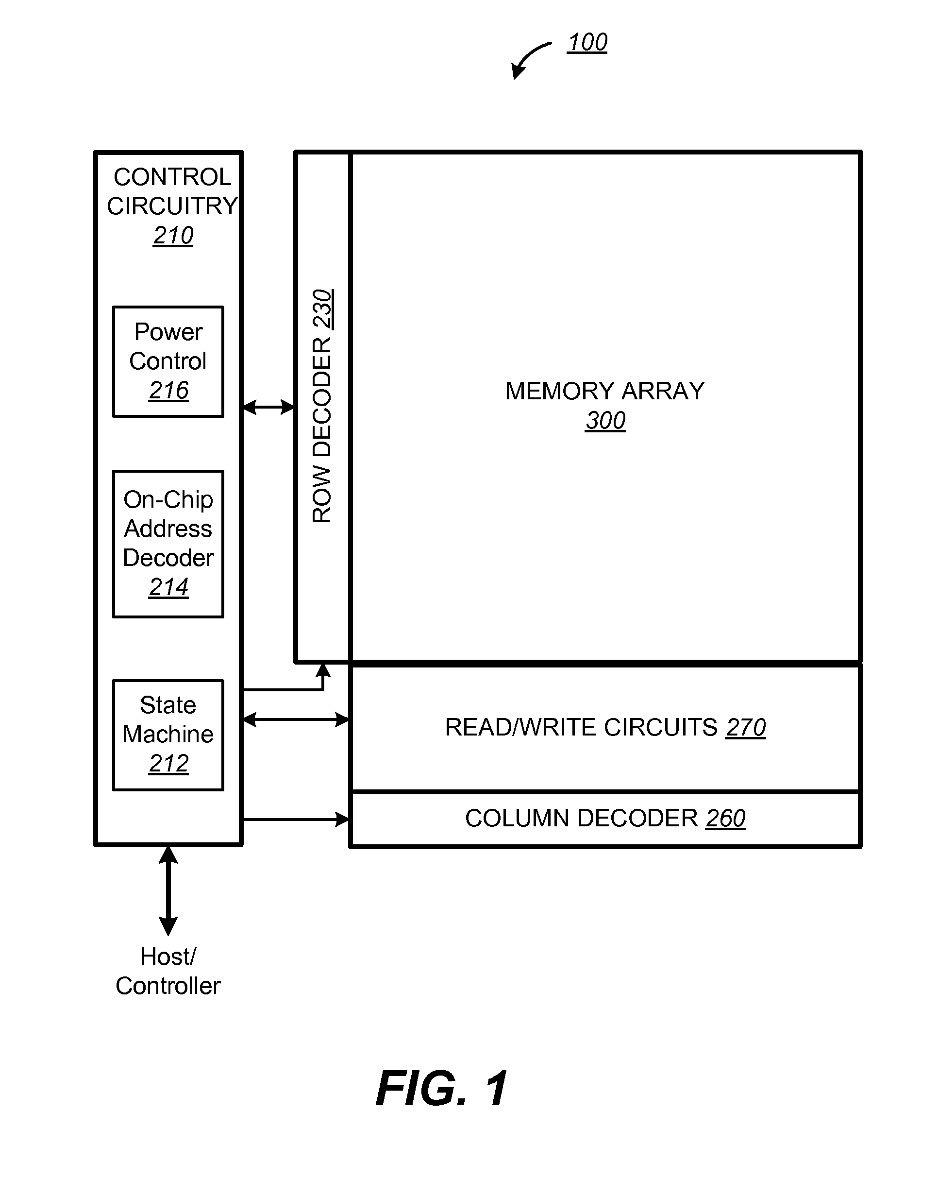
[0030]FIG. 1 illustrates schematically a compact memory device which provides the context in which the present invention is implemented. The memory device 100, usually in the form of a memory chip, includes a two-dimensional array of memory cells 300, control circuitry 210, and read / write circuits 270. The memory array 300 is addressable by word lines via a row decoder 230 and by bit lines via a column decoder 260. The read / write circuits 270 allow a page of memory cells to be read or programmed in parallel.
[0031]The control circuitry 210 cooperates with the read / write circuits 270 to perform memory operations on the memory array 300. It also interfaces with an external host or a memory controller to exchange. The control circuitry 210 includes a state machine 212, an on-chip address decoder 214 and a power control module 216. The state machine 212 provides chip level control of memory operations. The on-chip address decoder 214 provides an address interface between that used by the...
PUM
 Abstract
Description
Claims
Application Information