Auto-sequencing multi-directional inline processing apparatus

a processing apparatus and automatic sequence technology, applied in the field of system architecture, apparatus and method for processing substrates, can solve the problems of inability to use linear systems, complete system shutdown, and inability to manufacture whole systems, and achieve high throughput, high accuracy and throughput, and enabling detection and recovery of broken substrates

Active Publication Date: 2013-05-21
KLA CORP
View PDF40 Cites 13 Cited by
  • Summary
  • Abstract
  • Description
  • Claims
  • Application Information

AI Technical Summary

Benefits of technology

[0011]Various embodiments of the present invention provide a unique linear system architecture which can process silicon wafers of various sizes and can have high throughput. Various embodiments of the system provide apparatus and method for concurrent processing of several substrates at high accuracy and throughput, while enabling detection and recovery of broken substrates. The system employs a novel architecture which, while being linear, may autonomously sequence processing and move substrates in different directions as necessary. The system moves several substrates concurrently; however, unlike the prior art it does not utilize trays. Moreover, the system can also be used for processing individual large substrates of various materials.

Problems solved by technology

Recently, such flat panel fabrication systems have been modified for fabrication of thin film solar cells, albeit with limited success.
Conversely, in a linear architecture when one of the chambers is down, the entire system is shut down and cannot be used.
Also, linear system is not modular, in that the number of processing chambers cannot be easily changed once the system is set up.
Conversely, in a mainframe architecture, every time a process is completed in one chamber, the substrate must be picked up by the robotic arm and moved to another chamber, which adds transport overhead and reduces throughput.
Also, for systems that move wafers without a tray, breakage of a wafer can cause a shut down of the entire system for clean up and recovery.
The system moves several substrates concurrently; however, unlike the prior art it does not utilize trays.

Method used


Image

  • Auto-sequencing multi-directional inline processing apparatus
  • Auto-sequencing multi-directional inline processing apparatus
  • Auto-sequencing multi-directional inline processing apparatus

Examples


Embodiment Construction

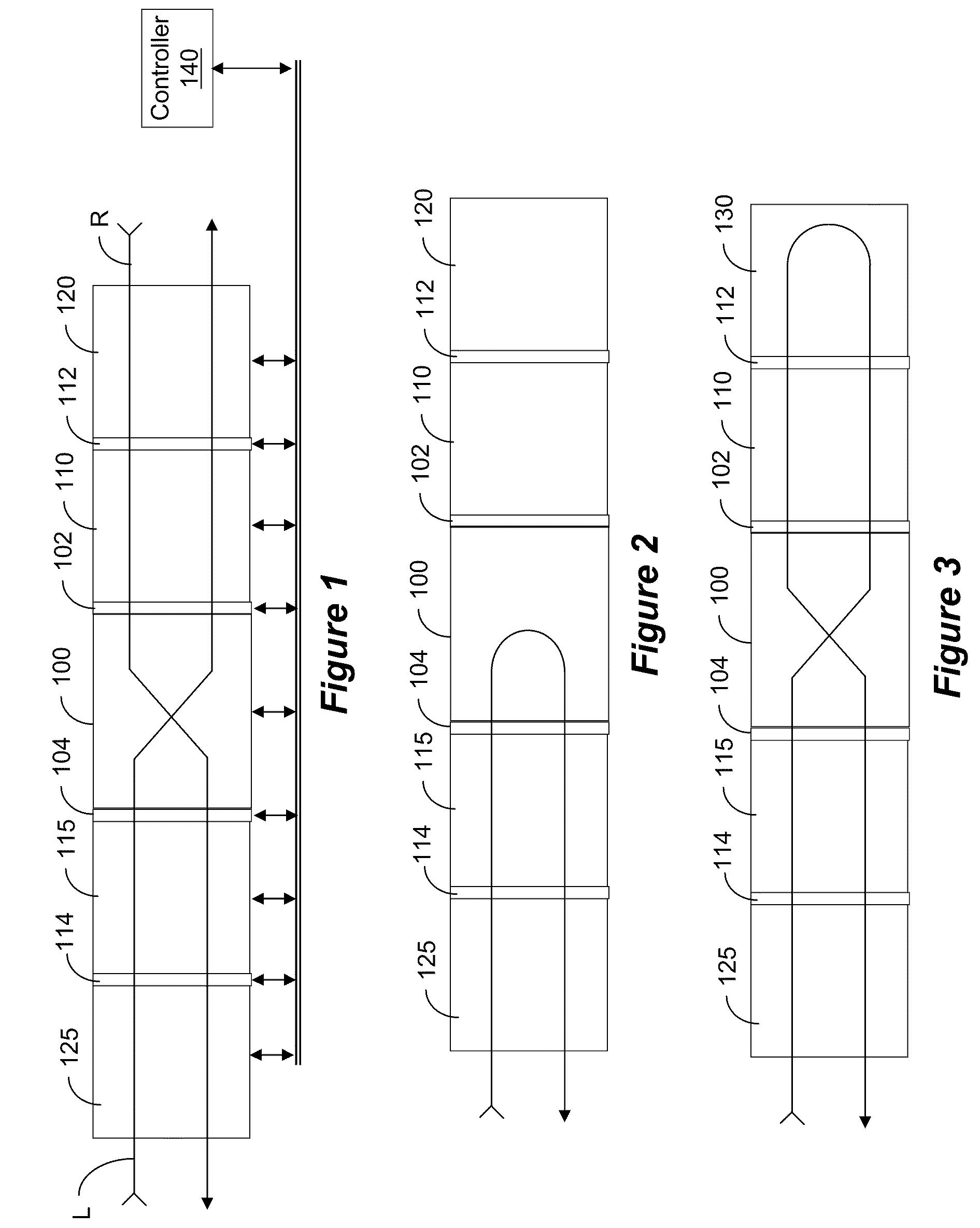
[0034]Various embodiments of the present invention provide apparatus and method for fabrication of substrates such as, e.g., for semiconductor integrated circuits, solar cells, flat panel displays, LED's and other applications. The system architecture is particularly beneficial for silicon-substrate solar cell fabrication and, therefore, for illustrative purpose will be described with reference to such application. The system sequences its transport of substrates and their fabrication autonomously, providing flexibility in feeding the system. This feature will be explained first in general terms with reference to FIGS. 1-3. More detailed explanation will follow further below.

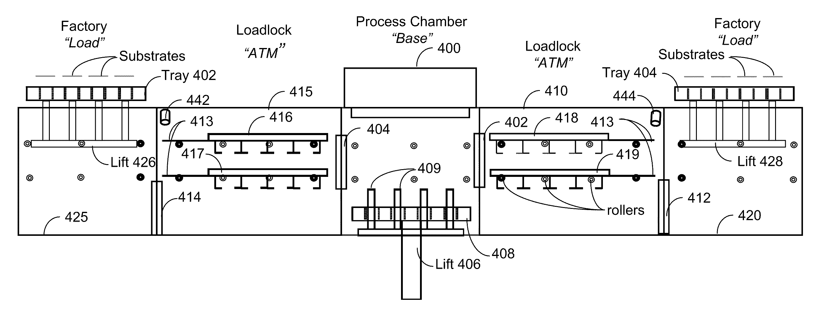
[0035]In FIG. 1, a single processing chamber 100 is situated at the center of the linear system. In this embodiment, the processing chamber is a plasma processing chamber such as, for example, a PECVD processing chamber. One vacuum valve, 102, 104, is provided on each side of the chamber 100. A loadlock chamber ...


PUM

PropertyMeasurementUnit
field of viewaaaaaaaaaa
atmospheric pressureaaaaaaaaaa
vacuumaaaaaaaaaa

Abstract

An apparatus and method for concurrent processing of several substrates. The system employs a novel architecture which, while being linear, may autonomously sequence processing and move substrates in different directions as necessary. The system moves several substrates concurrently; however, unlike the prior art it does not utilize trays.

Description

RELATED APPLICATIONS[0001]This application is a continuation of and claims priority from U.S. Provisional Application Ser. No. 61 / 285,505, filed on Dec. 10, 2009, the entire content of which is incorporated herein by reference.BACKGROUND[0002]1. Field of the Invention[0003]The present invention relates to system architecture, apparatus, and method for processing substrates in a clean environment, such as silicon wafers for semiconductor, solar cells, and other applications. The clean environment may be in vacuum or atmospheric pressure. The system can also be used with other substrates, such as glass for LCD and solar applications, stainless steel for thin film solar applications, etc.[0004]2. Description of the Related Art[0005]The photovoltaic (PV) solar cell industry can be roughly divided into two segments: thin film-based and silicon-wafer based PV cells. With the recent surge in demand for solar panels, various systems are currently being developed to enable high output manufa...

Claims


Application Information

Patent Timeline
Patent Type & Authority Patents(United States)
IPC IPC(8): B65G53/46
CPCC23C16/45565H01J37/32733H01L21/67745G06T7/0004H01L21/67754H01L21/67173H01L21/67748H01L21/67739Y10T29/49948H01J37/3244H01L21/02263H01L21/02274H01L21/3065H01L21/67207
Inventor BLONIGAN, WENDELL THOMASTOSHIMA, MASATOLAW, KAM S.BERKSTRESSER, DAVID ERICKLEINKE, STEVESTEVENS, CRAIG LYLE
Owner KLA CORP
Why Eureka
Try Eureka