
Scalable high-swing transmitter with rise and/or fall time mismatch compensation

Active Publication Date: 2013-05-21
MICROSEMI STORAGE SOLUTIONS
View PDF41 Cites 105 Cited by
  • Summary
  • Abstract
  • Description
  • Claims
  • Application Information

AI Technical Summary

Benefits of technology

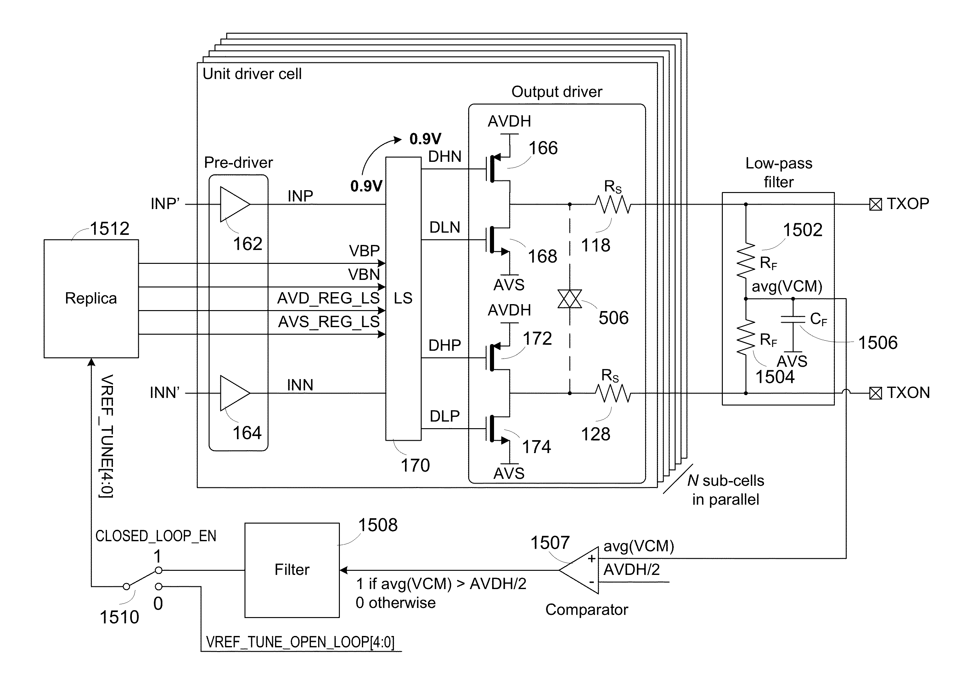
The invention helps reduce electromagnetic interference in a differential signal by matching the rise and fall times of a non-inverting portion and an inverting portion of the signal. This is done by tuning the pull-up and pull-down resistances. The higher launch amplitude allows for more equalization to compensate for printed circuit board and transmission channel losses, which allows for the use of cheaper PCB materials or longer PCB traces. The invention also includes a method of generating a differential output signal and a control circuit for optimizing the on resistance of PMOS and NMOS transistors in the output driver. This allows for better performance and improved rack-to-rack connectivity.

Problems solved by technology

One of the limiting factors for high-speed serial links is the band-limited response of the transmission medium (or channel) which causes increasing signal attenuation at high frequencies.
In addition, residual low-frequency signal energy from adjacent symbols can cause inter-symbol-interference (ISI), which can corrupt the “data eye” and lead to a reduced signal-to-noise ratio (SNR).
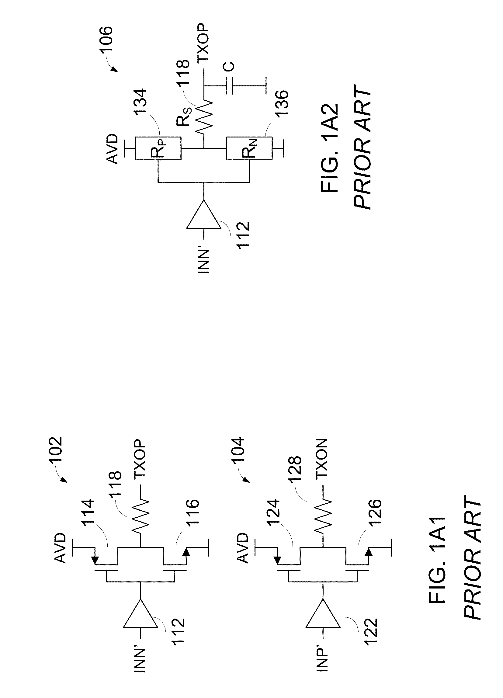
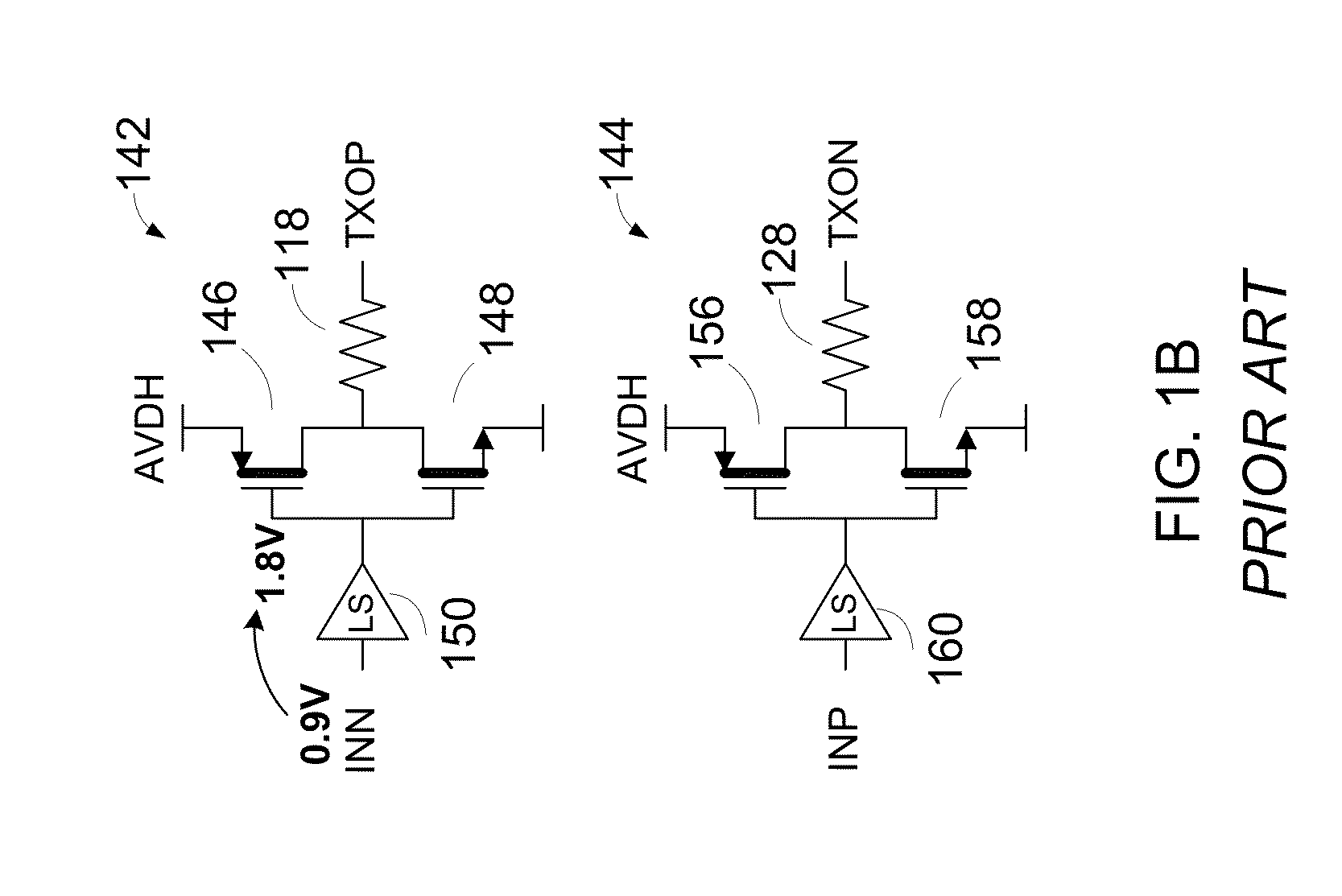
These advantages, however, come along with some drawbacks, such as relatively high static power consumption, headroom problems due to the lower supply voltage in newer technologies, and the inability to support different DC termination voltages as the output of the CML circuit is generally referenced to one of the two power supply rails.
This creates new design constraints, such as the desirability to interface a high-voltage output driver to a low-voltage pre-driver.
One problem that can occur with voltage-mode transmitters is electromagnetic interference (EMI).
EMI can be a difficult issue to resolve.
EMI requirements typically cannot be waived.
EMI compliance difficulties can lead to very expensive last minute shielding solutions or to expensive redesigns.

Method used


Image

  • Scalable high-swing transmitter with rise and/or fall time mismatch compensation
  • Scalable high-swing transmitter with rise and/or fall time mismatch compensation
  • Scalable high-swing transmitter with rise and/or fall time mismatch compensation

Examples


Embodiment Construction

[0074]Although particular embodiments are described herein, other embodiments of the invention, including embodiments that do not provide all of the benefits and features set forth herein, will be apparent to those of ordinary skill in the art.

[0075]In this description, reference is made to the drawings in which like reference numerals indicate identical or functionally similar elements.

[0076]The field-effect transistors (FETs) or “transistors” described herein can correspond to transistors known as metal-oxide-semiconductor field-effect transistors (MOSFETs). While the terms “metal” and “oxide” are present in the name of a MOSFET device, it will be understood that these transistors can have gates made out of materials other than metals, such as polysilicon, and that the dielectric oxide region can also be implemented not just with silicon dioxide, but with other dielectrics, such as high-k dielectrics. For example, reference in the description is made to “thin oxide” and to “thick ...


PUM


Abstract

Disclosed is a high-swing voltage-mode transmitter or line driver. The transmitter can operate over a wide range of supply voltages. Increasing the available output swing merely involves increasing the supply voltage; the circuit adapts to maintain the desired output impedance. This allows for a tradeoff between output amplitude and power consumption. Another advantage of the proposed architecture is that it compensates for process, voltage, and temperature (PVT) and mismatch variations so as to keep rise and fall times matched. This feature reduces common-mode noise and hence EMI in systems in which the transmitter is used.

Description

CROSS-REFERENCE TO RELATED APPLICATION[0001]This application claims the benefit under 35 U.S.C. §119(e) of U.S. Provisional Application No. 61 / 409,881, filed Nov. 3, 2010, the entirety of which is hereby incorporated by reference.[0002]This application is related to copending applications titled Apparatus and Method for Driving a Transistor, Ser. No. 13 / 288,866 and Apparatus and Method for Generating a Bias Voltage, Ser. No. 13 / 288,881, filed on the same date as the present application, the disclosure of which is hereby incorporated by reference in its entirety herein.BACKGROUND[0003]1. Field of the Invention[0004]The invention generally relates to electronics. In particular, the invention relates to wired transmitters or line drivers.[0005]2. Description of the Related Art[0006]The bandwidth requirements of networking and high-performance processing applications have been projected to continue to increase into the tens of giga bits per second (Gb / s) rates. For example, with referen...

Claims


Application Information

Patent Timeline
IPC IPC(8): H03K19/094
CPCH03K19/00361H03K17/162H03K17/145H03K19/00346H03K19/017509H03F3/2171
Inventor FAUCHER, JULIENVENDITTI, MICHAEL BEN
Owner MICROSEMI STORAGE SOLUTIONS
Learn More