Display device

a technology of display device and substrate, applied in the direction of radiation control device, dielectric characteristics, device details of semiconductor/solid-state device, etc., to achieve the effect of reducing the hardness and reducing the contact resistance between the substrate and the integrated circuit chip

Active Publication Date: 2013-06-18
SAMSUNG DISPLAY CO LTD
View PDF24 Cites 0 Cited by
  • Summary
  • Abstract
  • Description
  • Claims
  • Application Information

AI Technical Summary

Benefits of technology

[0011]Embodiments of the present invention to solve the above-described problem prevent the increase of the contact resistance between the substrate and the integrated circuit chip by fixing the compressed shape of the conductive balls.
[0027]According to the present invention, the pad unit includes the second conductive layer having the lesser hardness than the first conductive layer such that contact resistance between the substrate and the integrated circuit chip may be minimized.

Problems solved by technology

However, when pressure of more than a predetermined amount is applied to the conductive balls, the elastic restoring force of the compressed conductive halls exceeds the fixing capacity limit of the adhesive layer executing the adhesion between the substrate and the integrated circuit chip such that the adhesive layer does, not maintain the compressed shape of the conductive balls, and thereby the shape of the conductive balls is restored, and accordingly the contact resistance between the conductive balls and the pad, and the conductive balls and the terminal, is increased.

Method used


Image

  • Display device
  • Display device
  • Display device

Examples


Embodiment Construction

[0038]The present invention will be described more fully hereinafter with reference to the accompanying drawings, in which exemplary embodiments of the invention are shown. As those skilled in the art would realize, the described embodiments may be modified in various different ways, all without departing from the spirit or scope of the present invention.

[0039]The drawings and description are to be regarded as illustrative in nature and not restrictive. Like reference numerals designate like elements throughout the specification.

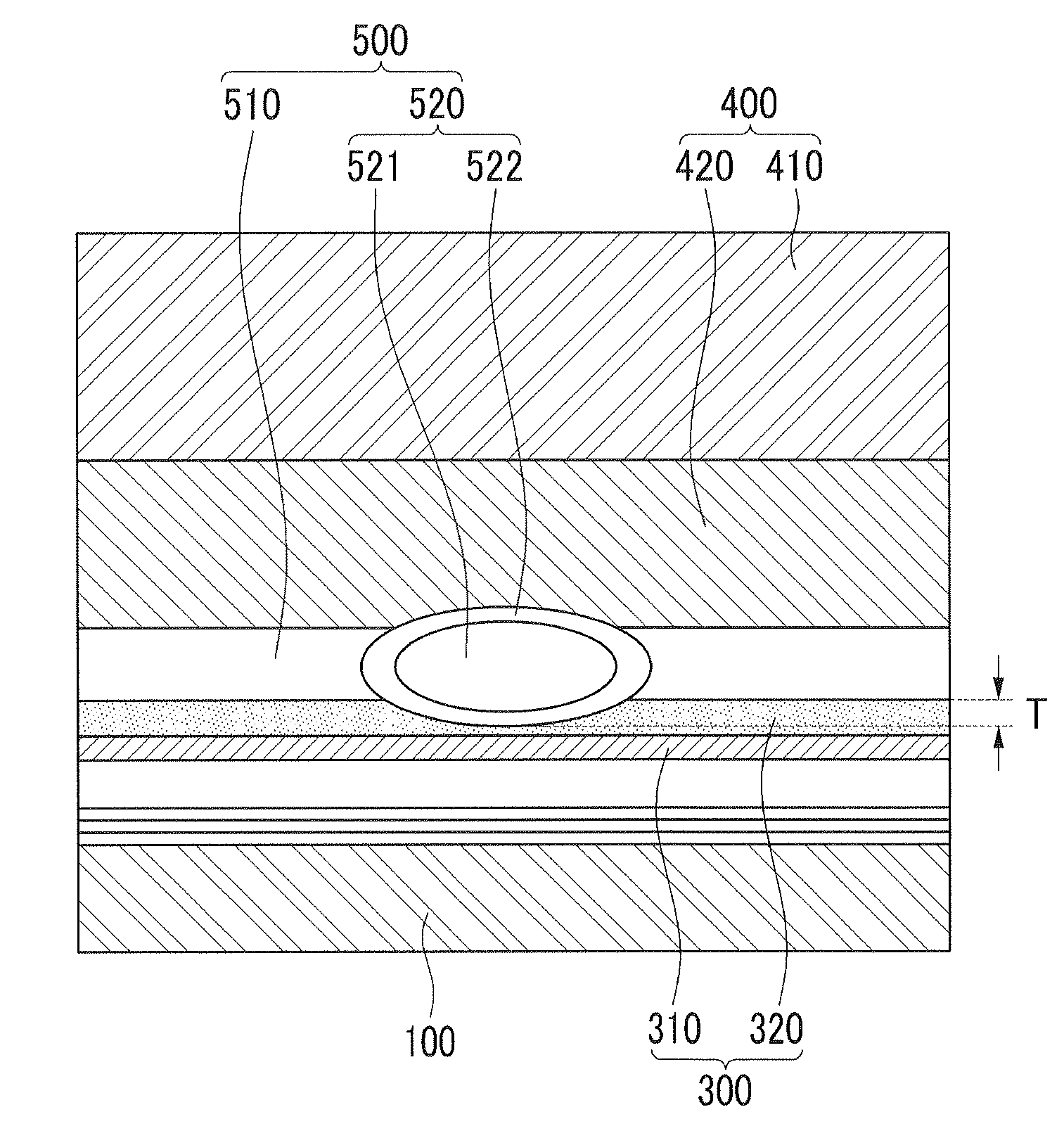
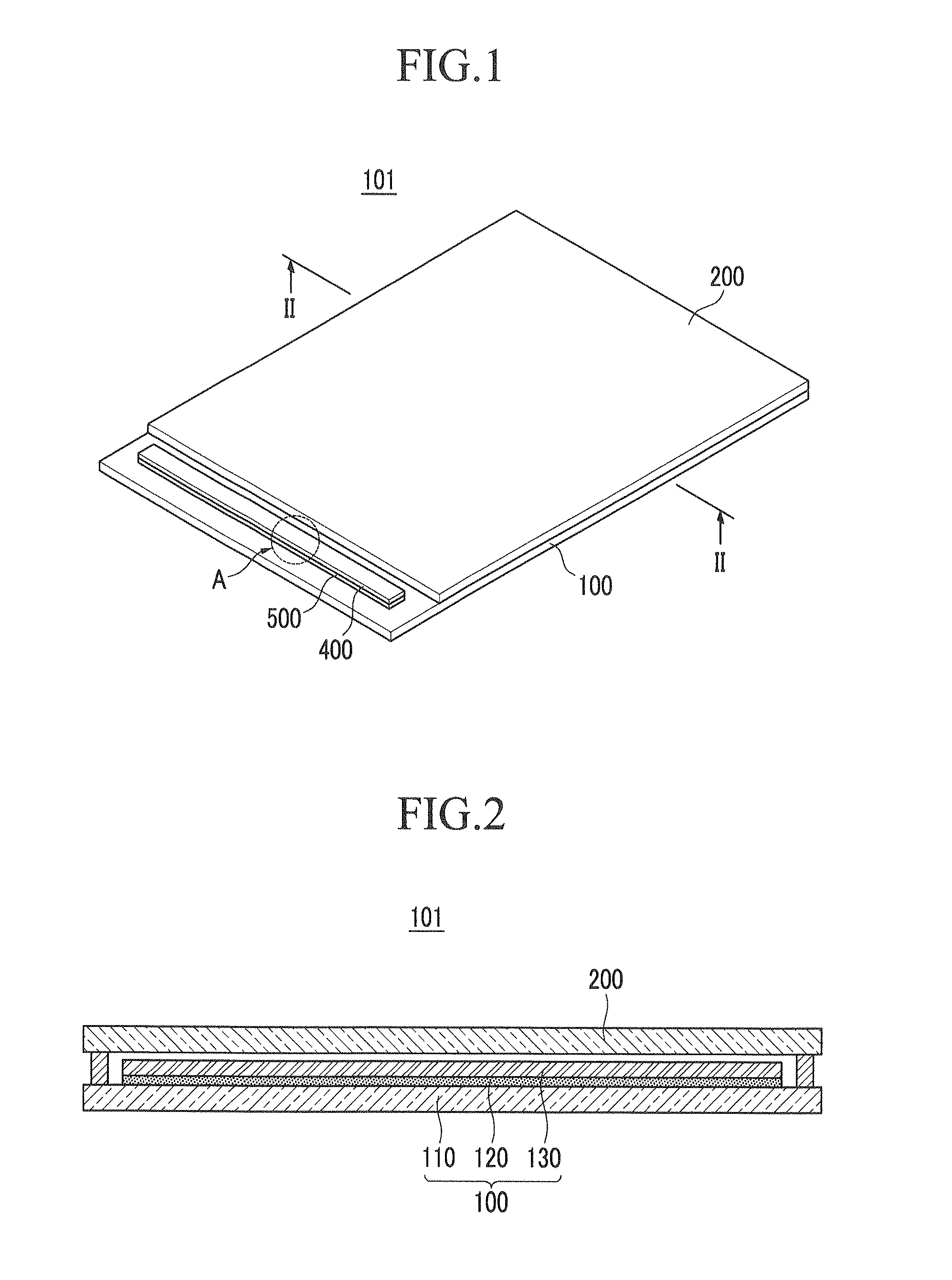
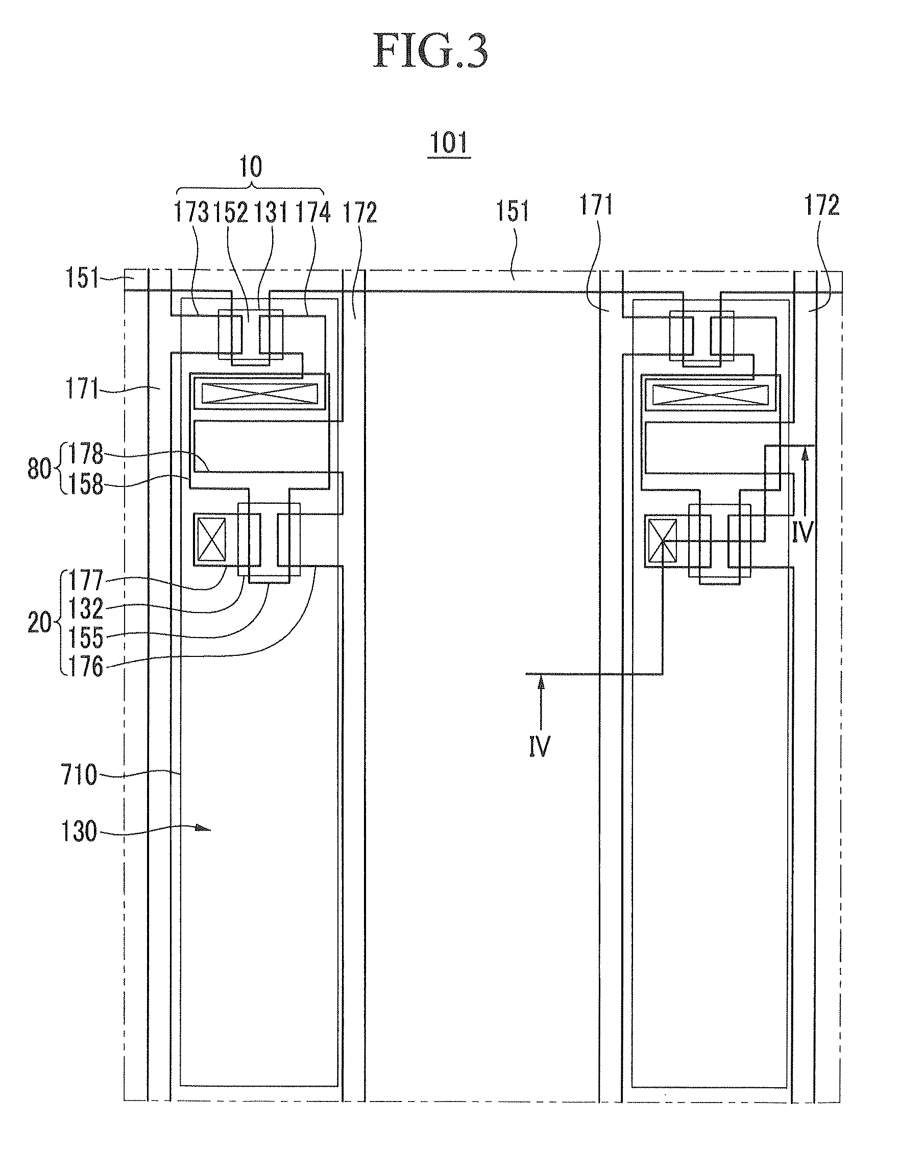
[0040]In order to clarify layers and regions, thicknesses and sizes thereof are exemplarily illustrated and thus the present invention is not limited thereto.

[0041]In the drawings, the thickness of layers, films, panels, regions, etc., are exaggerated for clarity. In addition, in order to clarify some layers and some regions, thicknesses and sizes thereof are enlarged in the drawings. It will be understood that when an element such as a layer, film, region, ...


PUM


Abstract

A display device includes a wire substrate including a wire unit for driving the display device, an integrated circuit chip mounted at the wire substrate, and a pad unit extended from the wire unit to be disposed between the wire substrate and the integrated circuit chip. The pad unit is connected to the integrated circuit chip. The pad unit includes a first conductive layer extended from the wire unit, and a second conductive layer disposed on the first conductive layer. The hardness of the second conductive layer is less than the hardness of the first conductive layer.

Description

CLAIM OF PRIORITY[0001]This application makes reference to, incorporates the same herein, and claims all benefits accruing under 35 U.S.C §119 from an application earlier filed in the Korean Intellectual Property Office on 2 Sep. 2009 and there duly assigned Ser. No. 10-2009-0082594.BACKGROUND OF THE INVENTION[0002]1. Field of the Invention[0003]The described technology relates generally to a display device. More particularly, the described technology relates generally to a display device mounted with an integrated circuit chip.[0004]2. Description of the Related Art[0005]As a display device for displaying images, an organic light emitting diode (OLED) display has recently been spotlighted.[0006]The OLED display has self-luminance characteristics, and the thickness and weight thereof can be reduced since a separate light source is not required, unlike a liquid crystal display (LCD). In addition, the OLED display has high-quality characteristics such as low power consumption, high lu...

Claims


Application Information

Patent Timeline
Patent Type & Authority Patents(United States)
IPC IPC(8): H01L27/14H05B44/00
CPCH01L27/3276H05K3/323H05K2201/0133H05K2201/0221H05K2201/0338H05K2201/10674H10K59/131H01L23/4922
Inventor LEELEE, CHOONG-HO
Owner SAMSUNG DISPLAY CO LTD
Why Eureka
Try Eureka