Light-emitting device

a light-emitting device and light-emitting technology, which is applied in the direction of static indicating devices, identification means, instruments, etc., can solve the problems of affecting the display of the light-emitting device by tfts, the effect of reducing the characteristics of transistors between different pixels, suppressing the luminance change accompanies deterioration of light-emitting elements or the lik

Inactive Publication Date: 2013-08-20
SEMICON ENERGY LAB CO LTD
View PDF77 Cites 16 Cited by
  • Summary
  • Abstract
  • Description
  • Claims
  • Application Information

AI Technical Summary

Benefits of technology

[0008]It is an object of the present invention to provide a light-emitting device which suppresses display unevenness. It is another object of the present invention to provide a light-emitting device in which variation in characteristics of transistors between different pixels is reduced. It is still another object of the present invention to provide a light-emitting device which suppresses decrease in luminance which accompanies deterioration of a light-emitting element or the like.
[0013]When a channel formation region of the transistor provided in the pixel is formed using a single-crystal semiconductor layer, a light-emitting device can be provided in which variation in characteristics of transistors between different pixels is reduced and thus display unevenness is suppressed. In the pixel, a channel formation region of the transistor connected to the light-emitting element is formed using a single-crystal semiconductor layer and the transistor is operated in the saturation region when the light-emitting element emits light. Accordingly, change in luminance which accompanies deterioration of the light-emitting element or the like can be suppressed.

Problems solved by technology

On the other hand, TFTs formed using polysilicon have a problem that electric characteristics are likely to vary between the TFTs due to defects at crystal grain boundaries.
Thus, luminance of light-emitting elements also varies, resulting in display unevenness in a light-emitting device.
However, as described above, there is a problem in that variation in characteristics of TFTs adversely affects display of the light-emitting device in the case where constant-current driving is performed using a TFT formed using polysilicon.
There is a problem in that luminance changes in accordance with a change in current since luminance of the light-emitting element is proportional to current.

Method used


Image

  • Light-emitting device
  • Light-emitting device
  • Light-emitting device

Examples


embodiment mode 1

[0056]This embodiment mode describes an example of the structure of a light-emitting device and a method for manufacturing the light-emitting device with reference to the drawings. A light-emitting device described in this embodiment mode uses an SOI (silicon on insulator) substrate. The SOI substrate can be formed by a bonding SOI technique. A light-emitting device manufactured using an SOI substrate in which a single-crystal semiconductor layer is bonded to a substrate having an insulating surface, such as glass, is described with reference to the drawings.

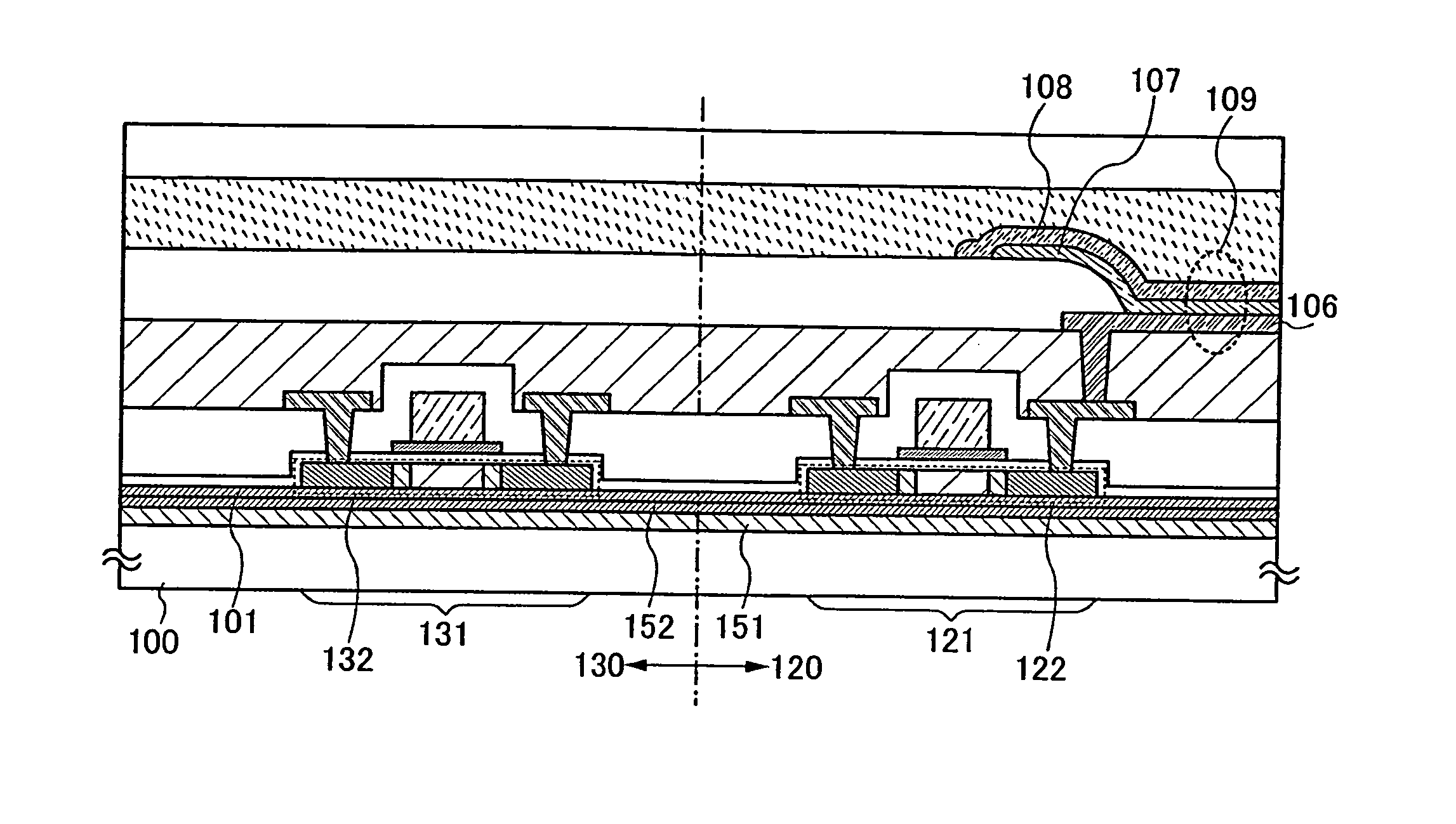
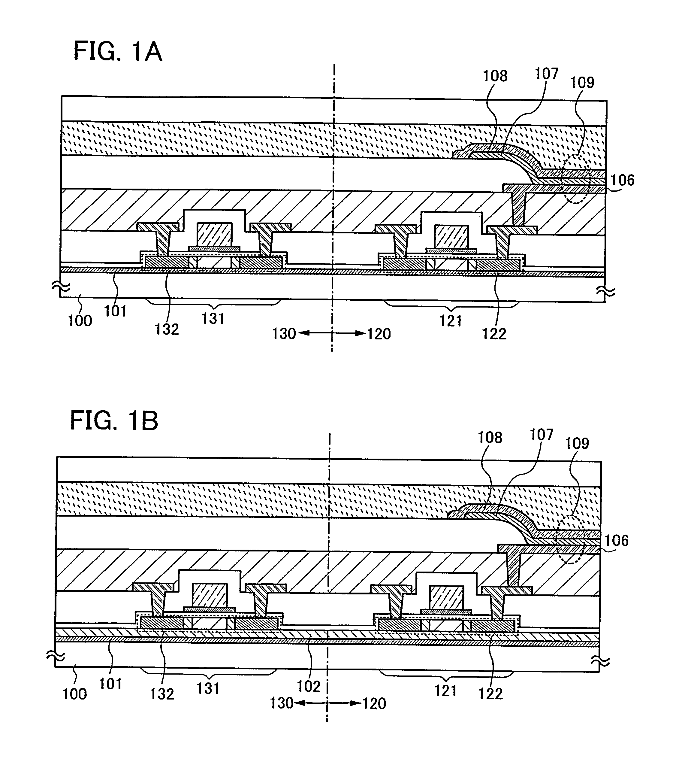
[0057]The structures of light-emitting devices in this embodiment mode are described with reference to FIGS. 1A and 1B. FIGS. 1A and 1B each show a pixel portion of a light-emitting device and a driver circuit portion which controls operation of the pixel portion.

[0058]A light-emitting device shown in FIG. 1A is provided with a transistor 121 included in a pixel portion 120 and a transistor 131 included in a driver circuit porti...

embodiment mode 2

[0160]This embodiment mode describes a method for manufacturing an SOI substrate, which is different from that in the above-described embodiment mode, with reference to the drawings.

[0161]First, a semiconductor substrate 161 is washed with a sulfuric acid / hydrogen peroxide mixture (SPM), an ammonia peroxide mixture (APM), a hydrochloric acid / hydrogen peroxide mixture (HPM), diluted hydrogen fluoride (DHF), or the like, as appropriate. Then, thermal oxidation of the semiconductor substrate 161 is performed to form an oxide film 190 (see FIG. 31A). Although the thermal oxidation may be conducted by dry oxidation, the thermal oxidation is preferably performed by oxidation in an oxygen atmosphere to which halogen is added. As a material including halogen, HCl is typical, and alternatively, one or more of HF, NF3, HBr, Cl2, ClF3, BCl3, F2, Br2, or the like can be used. As an example of such thermal oxidation, thermal oxidation may be conducted at 900 to 1150° C. (typically, 1000° C.) in ...

embodiment mode 3

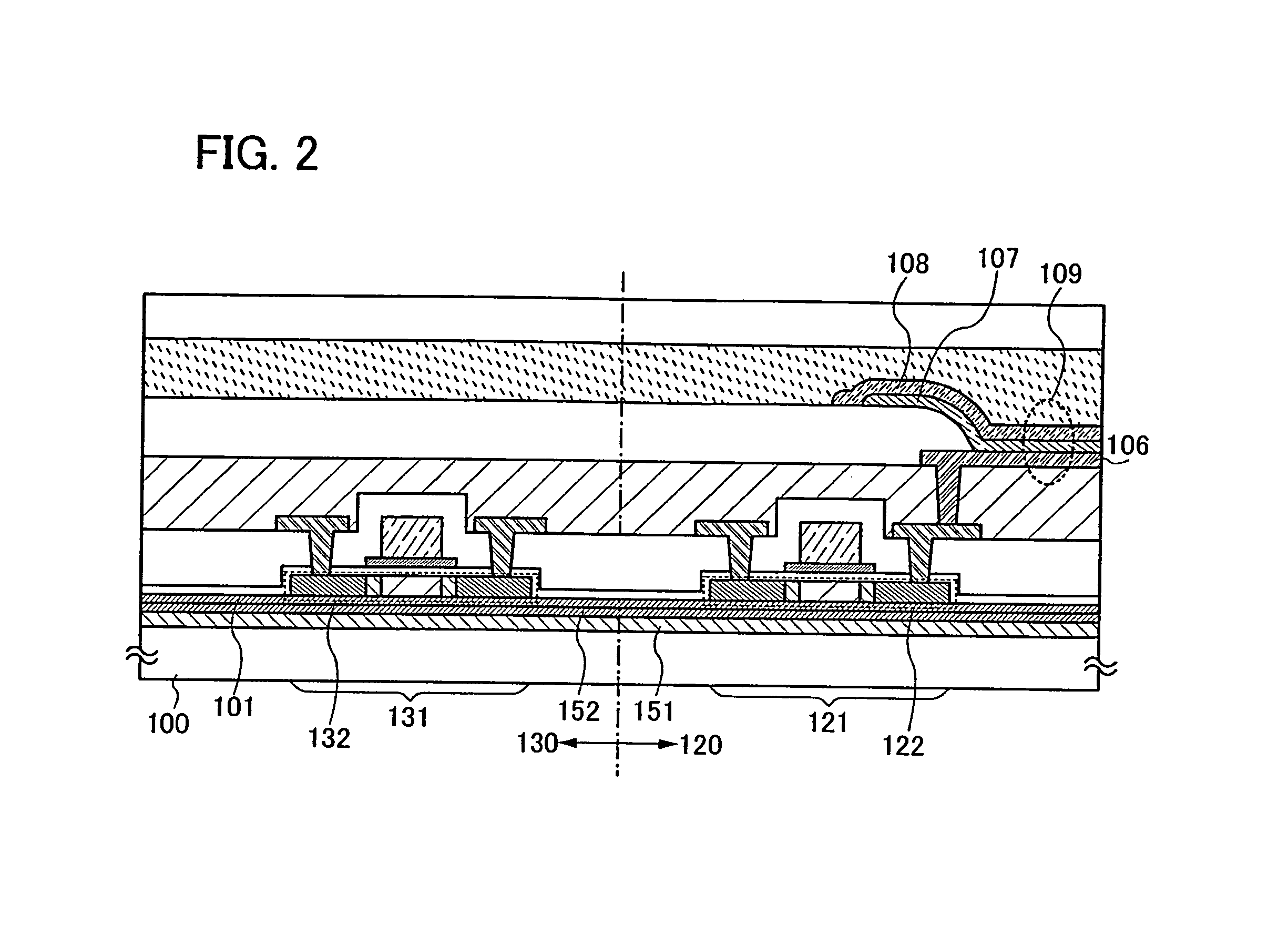
[0176]This embodiment mode describes an example of a light-emitting device with reference to the drawings.

[0177]FIG. 8 shows a block diagram of an active-matrix EL display device. The EL display device includes a driver circuit portion formed of a scanning line driver circuit 251, a signal line driver circuit 252, and the like, and a pixel portion 120 in which a plurality of pixels 253 is arranged.

[0178]A signal output from the signal line driver circuit 252 is input to signal lines S1 to Sx and transferred to each pixel 253. A signal output from the scanning line driver circuit 251 is input to scanning lines G1 to Gy and transferred to each pixel 253. Power supply lines V1 to Vx are arranged to be parallel to the signal lines and supply current to each pixel 253.

[0179]The EL display device described in this embodiment mode can have a structure in which the driver circuit portion including the scanning line driver circuit 251, the signal line driver circuit 252, and the like and the...


PUM


Abstract

A light-emitting device includes a pixel having a transistor provided over a substrate, and a light-emitting element. The transistor includes a single-crystal semiconductor layer which forms a channel formation region, a silicon oxide layer is provided between the substrate and the single-crystal semiconductor layer, a source or a drain of the transistor is electrically connected to an electrode of the light-emitting element, and the transistor is operated in a saturation region when the light-emitting element emits light. Further, in the light-emitting device, a gray scale of the light-emitting element is displayed by changing a potential applied to the gate of the transistor.

Description

BACKGROUND OF THE INVENTION[0001]1. Field of the Invention[0002]The present invention relates to a light-emitting device. In specific, the present invention relates to a light-emitting device in which a transistor included in a pixel uses a single-crystal semiconductor layer as a channel formation region.[0003]2. Description of the Related Art[0004]In recent years, technology to form a TFT over a substrate has greatly progressed, and application development for an active matrix display device has been promoted. In particular, since the field effect mobility (also called mobility) of a TFT using a polysilicon film is higher than that of a TFT using a conventional amorphous silicon film, high speed operation is possible. Therefore, development for controlling each pixel by providing a driver circuit including a TFT formed using a polysilicon film over the same substrate as the pixel is actively carried out. It is expected that, in an active matrix display device in which a driver circ...

Claims


Application Information

Patent Timeline
Patent Type & Authority Patents(United States)
IPC IPC(8): H01L33/00G09F9/30H01L21/02H01L21/336H01L21/8234H01L27/08H01L27/088H01L27/12H01L27/32H01L29/786H01L51/50
CPCG09G3/3208H01L27/1214H01L27/1266H01L33/02H01L29/66772H01L2924/0002H01L2924/00G09G3/20G09G3/30H01L27/12H10K59/38
Inventor YAMAZAKI, SHUNPEI
Owner SEMICON ENERGY LAB CO LTD
Why Eureka
Try Eureka