Method for producing group III nitride-based compound semiconductor, wafer including group III nitride-based compound semiconductor, and group III nitrided-based compound semiconductor device

a technology of nitride and compound semiconductor, which is applied in the direction of crystal growth process, polycrystalline material growth, chemically reactive gas growth, etc., can solve the problem of undesirable piezoelectric field generation attributed to internal strain

Active Publication Date: 2013-08-27
TOYODA GOSEI CO LTD
View PDF55 Cites 14 Cited by
  • Summary
  • Abstract
  • Description
  • Claims
  • Application Information

AI Technical Summary

Benefits of technology

[0027]Patent Document 1 discloses a technique in which, for example, mesas having a desired crystal growth surface are formed on a hetero-substrate (e.g., sapphire substrate) having a predetermined main surface; the surfaces other than the crystal growth surface are covered so that crystal growth does not occur on the surfaces; and, for example, a Group III nitride-based compound semiconductor is epitaxially grown so that the c-axis direction of the semiconductor is in a direction perpendicular to the crystal growth surface of the hetero-substrate; i.e., a desired axis-direction of the semiconductor is in a direction perpendicular to the main surface of the hetero-substrate.
[0028]Studies by the present inventors have shown that the technique disclosed in Non-Patent Document 1 merely allows epitaxial growth of a Group III nitride-based compound semiconductor on a sapphire substrate so that both c-plane and m-plane of the semiconductor are parallel to the main surface of the substrate.
[0029]Further studies by the present inventors have shown that when an aluminum thin film is formed on an a-plane main surface of a sapphire substrate having thereon a mesa having at least a side surface having an off-angle of 45° or less from c-plane, and then nitridation is carried out under optimized conditions, a Group III nitride-based compound semiconductor is formed so that m-plane of the semiconductor is parallel to the main surface of the sapphire substrate (fourth aspect).
[0030]Next will be described the mechanism of epitaxial growth through the aforementioned steps of the method provided by the present inventors.
[0031]FIGS. 1.A and 1.B show features of epitaxial growth carried out in the embodiments described hereinbelow. The mechanism of epitaxial growth will now be described with reference to FIGS. 1.A and 1.B. As shown in FIG. 1.A, hexagonal columnar (truncated hexagonal pyramidal) mesas are provided on an a-plane main surface of a sapphire substrate at appropriate intervals. FIG. 1.A shows the case where only one mesa is provided. As shown in FIG. 1.A, the hexagonal columnar (truncated hexagonal pyramidal) mesa has two side surfaces having an off-angle of 45° or less from c-plane (i.e., the gray side surface and the surface opposite thereto). The remaining side surfaces of the hexagonal columnar (truncated hexagonal pyramidal) mesa are not parallel or perpendicular to c-plane; i.e., the side surfaces are not c-plane, m-plane, or a-plane.
[0032]Studies by the present inventors have shown that when an aluminum thin film (thickness: 40 Å or less) is formed on a sapphire substrate having an a-plane main surface and having thereon a hexagonal columnar (truncated hexagonal pyramidal) mesa as shown in FIG. 1.A, and then the aluminum thin film is converted to an AlN film through nitridation, followed by epitaxial growth of a Group III nitride-based compound semiconductor, epitaxial growth of the semiconductor primarily occurs on the side surfaces of the mesa having an off-angle of 45° or less from c-plane so that the c-axis of the sapphire substrate corresponds to the c-axis of the semiconductor. In this case, rapid growth of the semiconductor does not occur on the remaining side surfaces of the mesa of the sapphire substrate, the a-plane top surface of the mesa of the sapphire substrate, or the non-mesa region of the sapphire substrate.

Problems solved by technology

Generation of such a piezoelectric field attributed to internal strain is also undesirable in the case of formation of a device other than a light-emitting device (e.g., HEMT).

Method used


Image

  • Method for producing group III nitride-based compound semiconductor, wafer including group III nitride-based compound semiconductor, and group III nitrided-based compound semiconductor device
  • Method for producing group III nitride-based compound semiconductor, wafer including group III nitride-based compound semiconductor, and group III nitrided-based compound semiconductor device
  • Method for producing group III nitride-based compound semiconductor, wafer including group III nitride-based compound semiconductor, and group III nitrided-based compound semiconductor device

Examples


embodiment 1

[0056]FIG. 2 schematically shows a specific embodiment of the method for producing a Group III nitride-based compound semiconductor of the present invention, which shows the temperature of a substrate, and supply / non-supply of raw materials or a carrier gas (hydrogen). Step numbers are given at the bottom of FIG. 2.

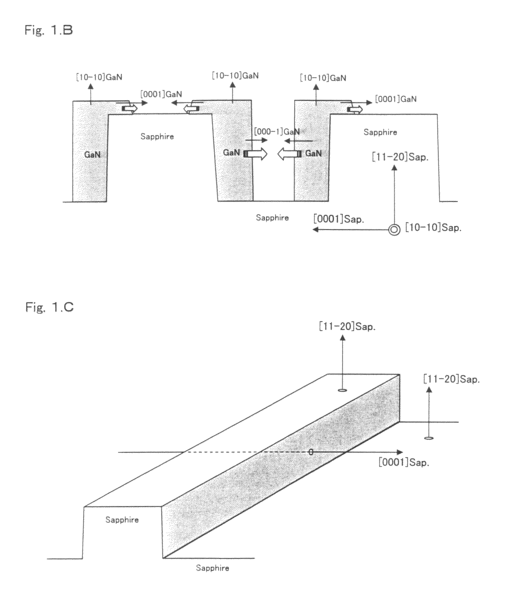
[0057]In step 1, in a hydrogen atmosphere, a sapphire substrate is heated to 1,160° C. and then cooled to 300 to 420° C.

[0058]In step 2, while the substrate is maintained at 300 to 420° C., trimethylaluminum is introduced under supply of a carrier gas (nitrogen-hydrogen mixture).

[0059]In step 3, introduction of trimethylaluminum is stopped, and the temperature of the substrate is elevated to 1,010° C. under supply of a carrier gas (nitrogen-hydrogen mixture) and ammonia.

[0060]In step 4, epitaxial growth is carried out through introduction of trimethylgallium under supply of a carrier gas (nitrogen-hydrogen mixture) and ammonia.

[0061]In step 5, the temperature of the subst...

embodiment 2

[0080]In Embodiment 2, the surface of a sapphire substrate was thermally treated without supply of trimethylaluminum; i.e., step 2 shown in FIG. 2 was omitted. That is, the surface of the sapphire substrate was thermally treated in a hydrogen atmosphere. Step 3 (nitridation) was initiated at 300 to 420° C. As a result, a relatively favorable Group III nitride-based compound semiconductor having an m-plane main surface was produced.

[0081]Even when, in step 1, cooling of the sapphire substrate was initiated at the moment when the substrate temperature reached 1,160° C. (i.e., the period during which the temperature of the sapphire substrate was maintained at 1,160° C. was zero), similar to the aforementioned case, a relatively favorable Group III nitride-based compound semiconductor having an m-plane main surface was produced.

embodiment 3

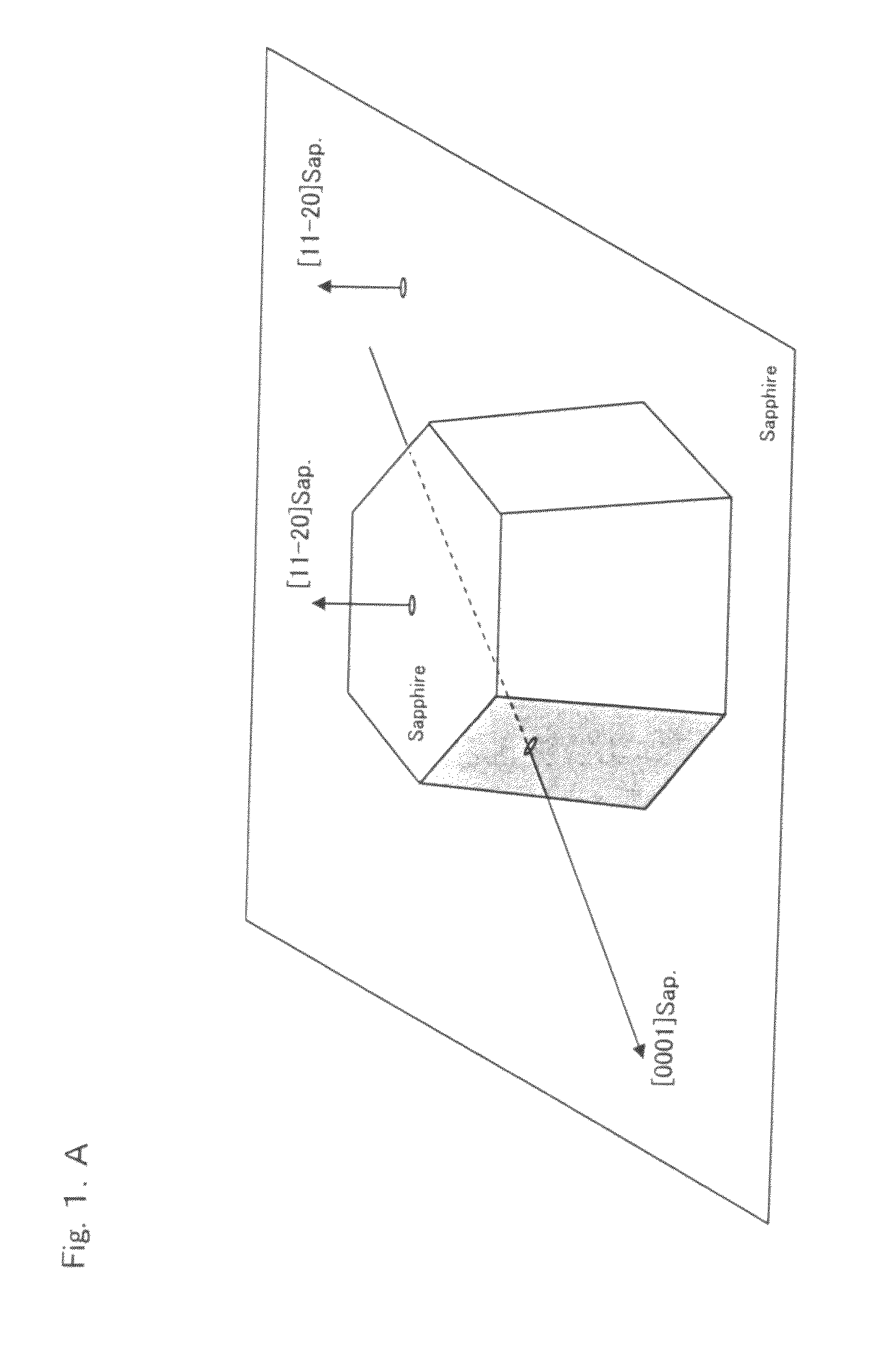
[0082]As described below, stripe-form mesas were formed on a sapphire substrate having an m-plane main surface. Specifically, the stripe-form mesas were formed so that the longitudinal direction thereof was inclined by 45° from the c-axis toward the a-axis in the main surface.

[0083]The stripe-form mesas were formed by use of an etching mask so that the width of each mesa (i.e., unetched portion) was 2 μm, and the distance between adjacent mesas (i.e., the width of an etched portion) was 3 μm. The etching depth was regulated to 0.7 μm. The angle between the m-plane main surface and side surfaces of each stripe-form mesa was about 70°.

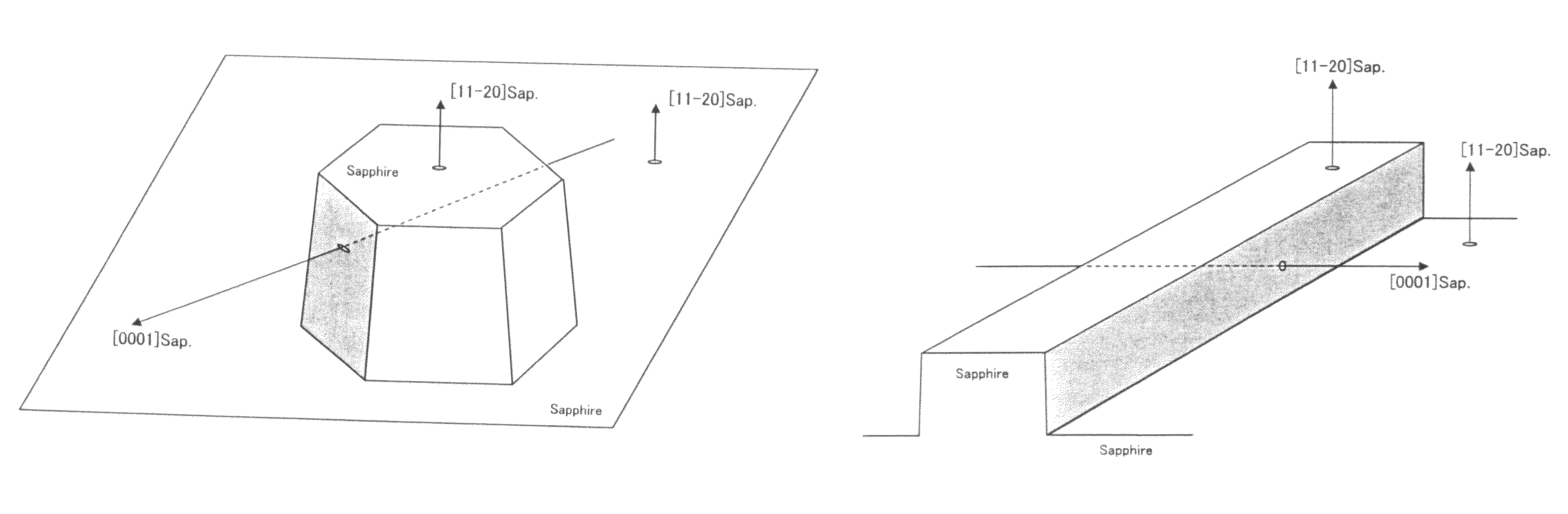
[0084]The m-plane sapphire substrate having the thus-formed mesas was treated in a manner similar to that described above in Embodiment 1, and then gallium nitride (Group III nitride-based compound semiconductor) was epitaxially grown, which is schematically shown in FIG. 6.

[0085]As shown in FIG. 6, a hexagonal columnar Group III nitride-based compound s...


PUM

PropertyMeasurementUnit
temperatureaaaaaaaaaa
off-angleaaaaaaaaaa
temperatureaaaaaaaaaa

Abstract

To produce a Group III nitride-based compound semiconductor having a m-plane main surface and uniformly oriented crystal axes.A mesa having a side surface having an off-angle of 45° or less from c-plane is formed in a a-plane main surface of a sapphire substrate. Subsequently, trimethylaluminum is supplied at 300° C. to 420° C., to thereby form an aluminum layer having a thickness of 40 Å or less. The aluminum layer is nitridated to form an aluminum nitride layer. Through the procedure, a Group III nitride-based compound semiconductor is epitaxially grown only from a side surface of the mesa having an off-angle of 45° or less from c-plane in the sapphire substrate having an a-plane main surface. Thus, a Group III nitride-based compound semiconductor having m-plane which is parallel to the main surface of the sapphire substrate can be formed.

Description

TECHNICAL FIELD[0001]The present invention relates to a method for producing a Group III nitride-based compound semiconductor having a so-called wurtzite structure. More particularly, the present invention relates to a method for producing, through epitaxial growth, a Group III nitride-based compound semiconductor having an m-plane main surface.[0002]As used herein, “Group III nitride-based compound semiconductor” encompasses a semiconductor represented by the formula AlxGayIn1-x-yN (0≦x≦1, 0≦1, 0≦x+y≦1); such a semiconductor containing a predetermined element so as to attain, for example, an n-type / p-type conduction; and such a semiconductor in which a portion of a Group III element is substituted by B and / or Ti, and / or a portion of the Group V element is substituted by P, As, Sb, and / or Bi.BACKGROUND ART[0003]Group III nitride-based compound semiconductor light-emitting devices have been widely used, and many attempts have been made to improve characteristics of the devices. In ge...

Claims


Application Information

Patent Timeline
Patent Type & Authority Patents(United States)
IPC IPC(8): H01L29/20H01L21/20C30B25/18C30B29/38
CPCC30B25/18C30B29/403H01L21/0242H01L21/02433H01L21/02609H01L21/0262H01L21/0254H01L33/007H01L21/02658
Inventor OKUNO, KOJINITTA, SHUGOSAITO, YOSHIKIUSHIDA, YASUHISANAKADA, NAOYUKIBOYAMA, SHINYA
Owner TOYODA GOSEI CO LTD
Why Eureka
Try Eureka