Solid-state imaging device, imaging apparatus, and method for manufacturing solid-state imaging device

a solid-state imaging and imaging device technology, applied in the field of solid-state imaging devices, imaging apparatus, and manufacturing solid-state imaging devices, can solve the problems of generating streaky fixed pattern noise in scanned images, a-si is not suitable for high-sensitivity image sensors, and it is not possible to manufacture sensors having the diameter of silicon wafers. large, high-speed reading

Inactive Publication Date: 2013-09-24
FUJIFILM CORP
View PDF17 Cites 178 Cited by
  • Summary
  • Abstract
  • Description
  • Claims
  • Application Information

AI Technical Summary

Benefits of technology

[0017]An object of the invention is to provide a solid-state imaging device in which a fixed pattern noise is not generated, an optical system for connection is not needed, and high sensitivity, high-speed reading, large size, and low cost can be realized.

Problems solved by technology

However, in an actual semiconductor process using a silicon wafer, a plurality of image sensors are used in a connected state because an image sensor having a size larger than a wafer size (currently, maximum 300 mm in diameter) cannot be manufactured.
This generates a streaky fixed pattern noise in a scanned image.
Accordingly, the a-Si is not suitable for an image sensor for high sensitivity, high-speed reading, and high S / N.
Although a CCD or a CMOS sensor is excellent in terms of high sensitivity and high-speed reading since the CCD or the CMOS sensor is formed of single crystal silicon, it is not possible to manufacture a sensor having a diameter of a silicon wafer, currently, a sensor having a size of maximum 12 inches (300 mm) because a silicon wafer is manufactured as a substrate.
In this case, however, high-speed reading cannot be expected theoretically since the mobility of electron and hole in the amorphous silicon is equal to or smaller than 1 / 100 of that of single crystal silicon.
A problem of a connection type sensor lies in a connecting method.
Although the CCD or CMOS is configured to include a plurality of photodiodes arrayed and a signal readout circuit that is connected to each of the photodiodes and reads a signal charge in a sequential manner, the photodiodes and the signal readout circuit cannot be formed up to the approximate end of a chip surface (since the performance deteriorates due to an influence of the chip end surface).
Accordingly, even if elements are arrayed with mechanically high accuracy, a sensitivity difference or a black level difference occurs in a connection portion of the elements, resulting in a fixed pattern noise.
Although the fixed pattern noise can be suppressed by a signal processing circuit, the cost increases in the case.
Although the connection type sensor has the high sensitivity and performs high-speed reading as described above, there were disadvantages in that the cost for the connection increased and an imaging optical system was made large.
However, it was almost impossible to array pixels on the end surfaces in the four directions.

Method used


Image

  • Solid-state imaging device, imaging apparatus, and method for manufacturing solid-state imaging device
  • Solid-state imaging device, imaging apparatus, and method for manufacturing solid-state imaging device
  • Solid-state imaging device, imaging apparatus, and method for manufacturing solid-state imaging device

Examples


first embodiment

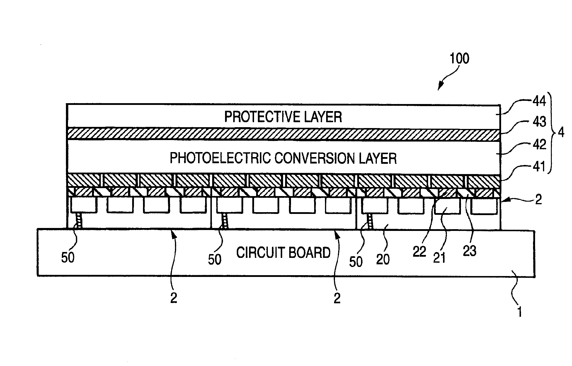
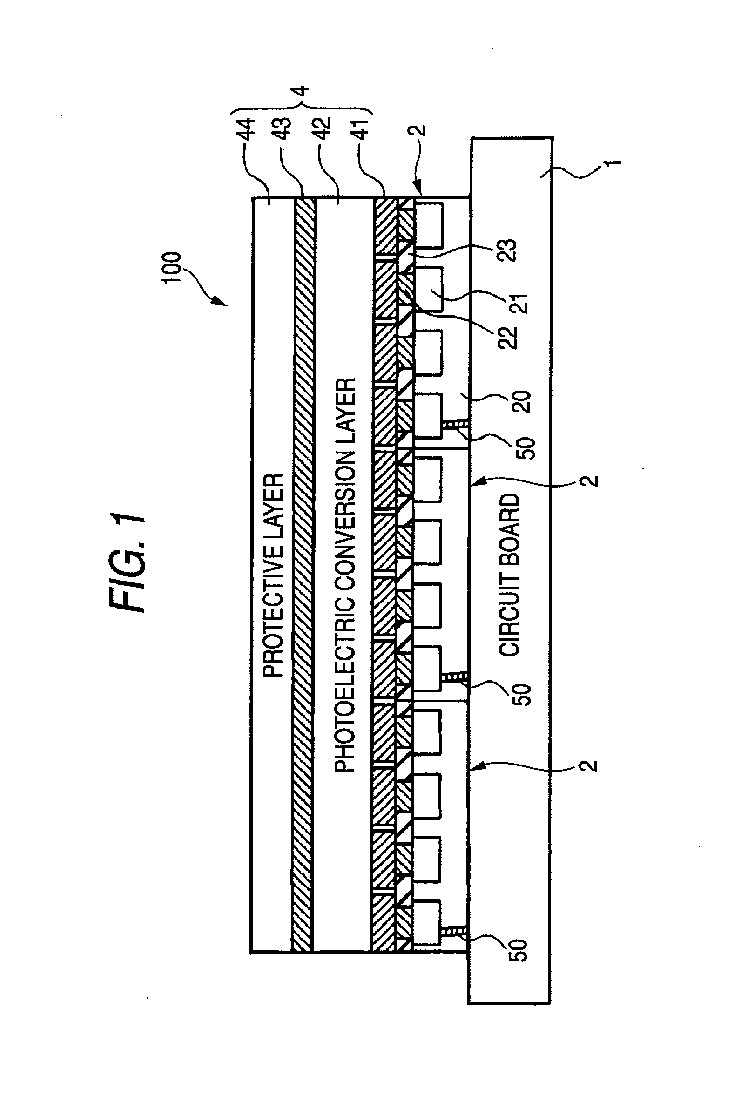
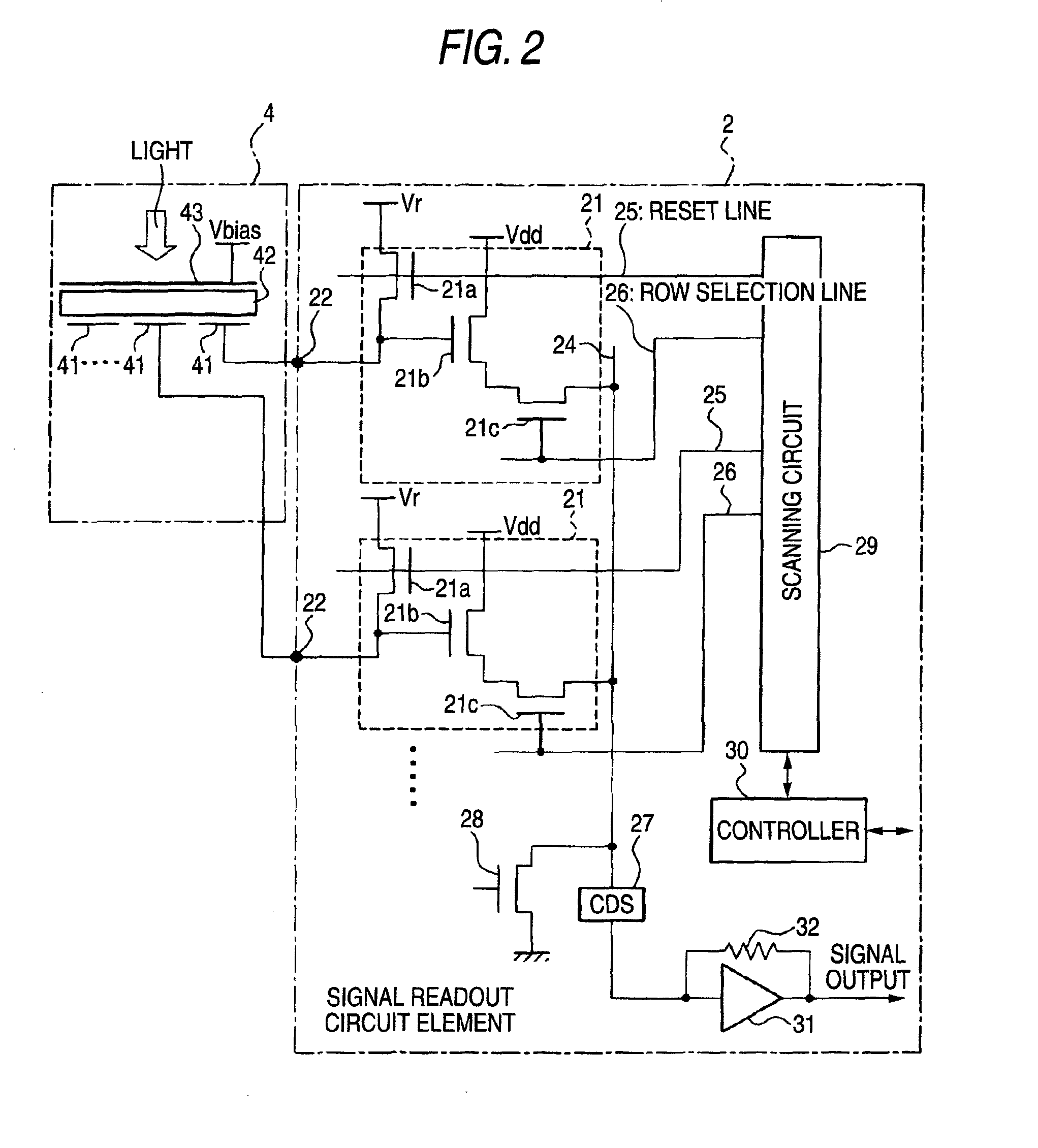
[0059]FIG. 1 is a cross-sectional view showing the schematic configuration of a solid-state imaging device according to a first exemplary embodiment of the invention. FIG. 2 is a circuit diagram showing the detailed configuration of a signal readout circuit element 2 shown in FIG. 1. FIG. 3 is a mimetic diagram showing the entire configuration of the solid-state imaging device shown in FIG. 1.

[0060]The solid-state imaging device 100 shown in FIG. 1 includes a circuit board 1, a plurality of signal readout circuit elements 2 arranged in a one-dimensional manner on the circuit board 1 as shown in FIG. 3, and a photoelectric conversion section 4 formed on the plurality of signal readout circuit elements 2.

[0061]The photoelectric conversion section 4 includes a plurality of pixel electrodes 41 arrayed in a one-dimensional manner, a photoelectric conversion layer 42 which has a one-sheet configuration and is formed on the plurality of pixel electrodes 41, a opposite electrode 43 which ha...

second embodiment

[0093]In a solid-state imaging device described in a second exemplary embodiment, the array of the signal readout circuit elements 2 of the solid-state imaging device 100 described in the first embodiment is changed from the one-dimensional shape to the two-dimensional shape, the array of photoelectric conversion elements corresponding to the respective signal readout circuit element 2 is changed from the one-dimensional shape to the two-dimensional shape, and the configuration of each signal readout circuit element 2 and the configuration of the circuit board 1 change with the changes.

[0094]FIG. 5 is a schematic view showing the entire configuration of a solid-state imaging device 200 according to a second embodiment of the invention. FIG. 6 is a plan view schematically showing the solid-state imaging device 200 according to the second embodiment of the invention. FIG. 7 is a circuit diagram showing the detailed configuration of a signal readout circuit element 2 shown in FIG. 6. T...


PUM


Abstract

A solid-state imaging device is provided and includes: a substrate; a plurality of photoelectric conversion elements arranged in a one-dimensional or two-dimensional array above the substrate, the plurality of photoelectric conversion elements being divided into a plurality of photoelectric conversion element groups; a plurality of semiconductor substrates between the substrate and the plurality of photoelectric conversion elements, each of the plurality of semiconductor substrates corresponding to each of the plurality of photoelectric conversion element groups; and a signal output section in the plurality of semiconductor substrates. The signal output section outputs a signal corresponding to an electric charge generated in each photoelectric conversion elements of a photoelectric conversion element group corresponding to a semiconductor substrate.

Description

[0001]This application is based on and claims priority under 35 U.S.C. §119 from Japanese Patent Application No. 2007-263205 filed Oct. 9, 2007, the entire disclosure of which is herein incorporated by reference.BACKGROUND OF THE INVENTION[0002]1. Field of the Invention[0003]The present invention relates to a solid-state imaging device having a plurality of photoelectric conversion elements arranged in a one-dimensional or two-dimensional array above a substrate.[0004]2. Description of Related Art[0005]A one-dimensional image sensor that reads a document in a state almost in contact with the document and in a condition where a read width is set equal to an original document width, a so-called same size and contact type line sensor is widely used for a document scanner of a copying machine or a FAX. In the case of the same size and contact type line sensor, miniaturization of a scanner and reduction in cost are expected since an optical system which forms a document image on an image...

Claims


Application Information

Patent Timeline
Patent Type & Authority Patents(United States)
IPC IPC(8): H01L27/00H01J40/14
CPCH01L27/14634H01L27/14667H04N5/3692H04N5/3742H04N5/376H04N25/701H04N25/767H04N25/74
Inventor INUIYA, MASAFUMI
Owner FUJIFILM CORP
Why Eureka
Try Eureka