Semiconductor integrated circuit

a technology of integrated circuits and semiconductors, applied in the direction of power consumption reduction, pulse techniques, instruments, etc., can solve the problems of reducing the effect of power gating on reducing power consumption, reducing the efficiency of semiconductor integrated circuits, and so as to reduce the delay of operation and power consumption. , the effect of reducing the delay of operation

Inactive Publication Date: 2013-10-01
SEMICON ENERGY LAB CO LTD
View PDF158 Cites 206 Cited by
  • Summary
  • Abstract
  • Description
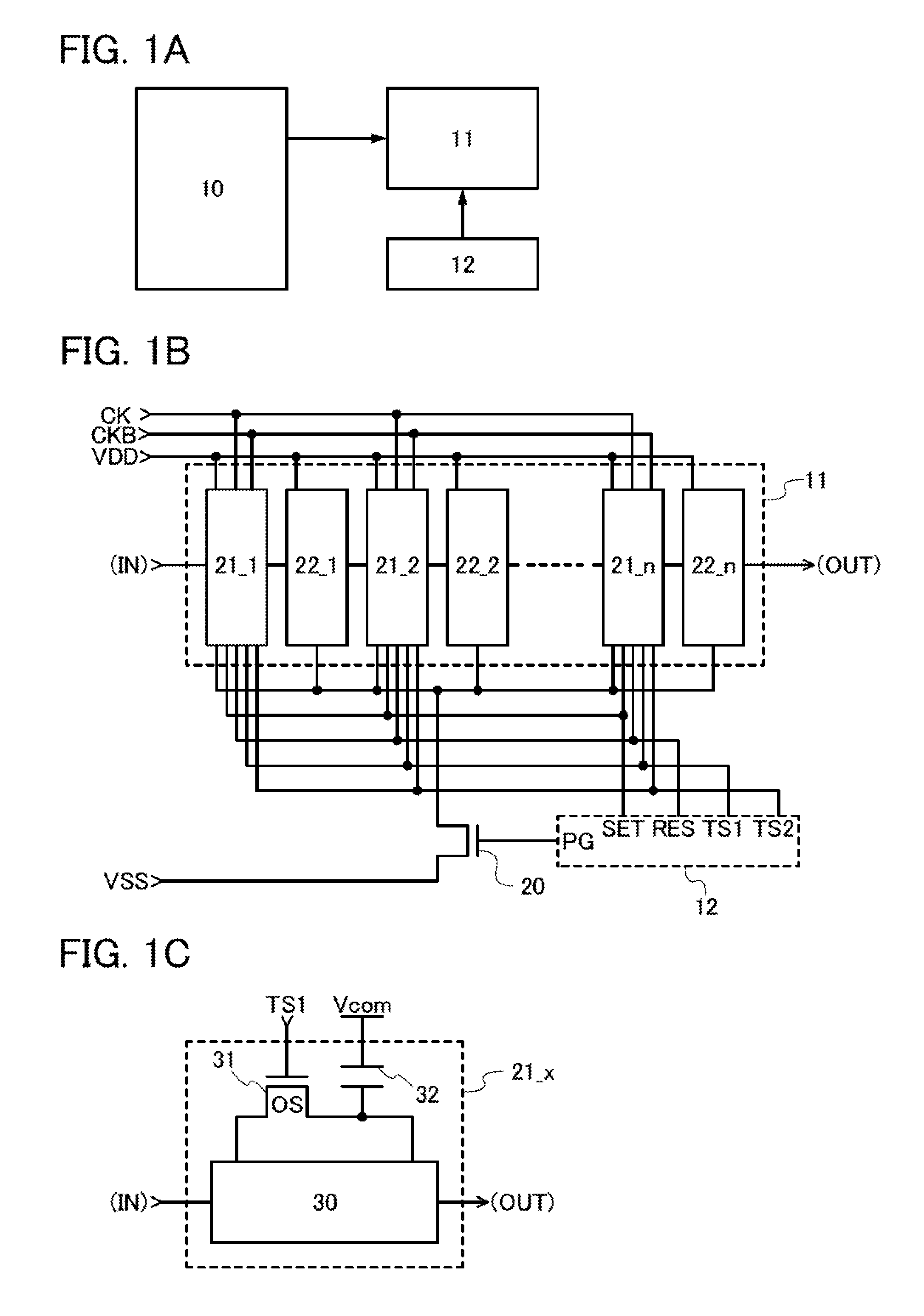
  • Claims
  • Application Information

AI Technical Summary

Benefits of technology

[0007]In view of the foregoing problems, an object of one embodiment of the present invention is to reduce power consumption of a semiconductor integrated circuit. Another object of one embodiment of the present invention is to reduce delay of the operation in a semiconductor integrated circuit. Note that one embodiment of the present invention aims to achieve at least one of the above objects.
[0008]At least one of the above objects can be achieved as follows: a plurality of sequential circuits included in a storage circuit each include a transistor whose channel formation region is formed with an oxide semiconductor, and a capacitor whose one electrode is electrically connected to a node that is brought into a floating state when the transistor is turned off. The oxide semiconductor has a band gap wider than silicon and an intrinsic carrier density lower than silicon. By using such an oxide semiconductor for a channel formation region of the transistor, the transistor with an extremely low off-state current (leakage current) can be realized. Thus, by turning off the transistor in a period during which power supply voltage is not supplied to the storage circuit, the potential in that period of the node to which one electrode of the capacitor is electrically connected can be kept constant or almost constant. As a result, arithmetic operation or the like does not need to be performed again when supply of power supply voltage to the storage circuit is restarted. In other words, in the semiconductor integrated circuit according to one embodiment of the present invention, there is no power consumption nor delay of the operation due to the additional arithmetic operation, which means that the above object can be achieved.
[0013]In a semiconductor integrated circuit according to one embodiment of the present invention, the potential of a specific node can be held in each of a plurality of sequential circuits included in a storage circuit even in a period when power supply voltage is not supplied to the storage circuit. In addition, the potential held in the node can be matched to data held in the sequential circuit. In other words, in the semiconductor integrated circuit according to one embodiment of the present invention, arithmetic operation or the like does not need to be performed on the storage circuit when supply of power supply voltage is started again. Thus, power consumption can be reduced and delay of the operation can be reduced in the semiconductor integrated circuit according to one embodiment of the present invention.

Problems solved by technology

In fact, it is common knowledge that storage circuits such as registers are frequently used in logic circuits included in existing semiconductor integrated circuits, and power gating causes erasing of stored data.
For that reason, the effect of reducing power consumption due to power gating is weakened.
Further, the operation of the semiconductor integrated circuit cannot be restarted until the arithmetic operation is completed, so that the operation of the semiconductor integrated circuit is delayed.

Method used


Image

  • Semiconductor integrated circuit
  • Semiconductor integrated circuit
  • Semiconductor integrated circuit

Examples


example 1

[0299]The actually measured field-effect mobility of an insulated gate transistor can be lower than its original mobility because of a variety of reasons; this phenomenon occurs not only in the case of using an oxide semiconductor. One of the reasons that reduce the mobility is a defect inside a semiconductor or a defect at an interface between the semiconductor and an insulating film. When a Levinson model is used, the field-effect mobility that is based on the assumption that no defect exists inside the semiconductor can be calculated theoretically.

[0300]Assuming that the original mobility and the measured field-effect mobility of a semiconductor are μ0 and μ, respectively, and a potential barrier (such as a grain boundary) exists in the semiconductor, the measured field-effect mobility μ can be expressed as the following formula.

[0301]μ=μ0⁢exp⁡(-EkT)[Formula⁢⁢5]

[0302]Here, E represents the height of the potential barrier, k represents the Boltzmann constant, and T represents the ...

example 2

[0362]In this example, an example of a transistor in which an In—Sn—Zn—O film is used as an oxide semiconductor film will be described with reference to FIGS. 38A and 38B.

[0363]FIGS. 38A and 38B are a top view and a cross-sectional view of a coplanar transistor having a top-gate top-contact structure. FIG. 38A is the top view of the transistor. FIG. 38B illustrates cross section A-B along dashed-dotted line A-B in FIG. 38A.

[0364]The transistor illustrated in FIG. 38B includes a substrate 600; a base insulating film 602 provided over the substrate 600; a protective insulating film 604 provided in the periphery of the base insulating film 602; an oxide semiconductor film 606 that is provided over the base insulating film 602 and the protective insulating film 604 and includes a high-resistance region 606a and low-resistance regions 606b; a gate insulating layer 608 provided over the oxide semiconductor film 606; a gate layer 610 provided to overlap with the oxide semiconductor film 60...

example 3

[0366]In this example, another example of a transistor in which an In—Sn—Zn—O film is used as an oxide semiconductor film will be described.

[0367]FIGS. 39A and 39B are a top view and a cross-sectional view illustrating a structure of a transistor. FIG. 39A is the top view of the transistor. FIG. 39B is a cross-sectional view along dashed-dotted line A-B in FIG. 39A.

[0368]The transistor illustrated in FIG. 39B includes a substrate 700; a base insulating film 702 provided over the substrate 700; an oxide semiconductor film 706 provided over the base insulating film 702; a pair of electrodes 714 in contact with the oxide semiconductor film 706; a gate insulating layer 708 provided over the oxide semiconductor film 706 and the pair of electrodes 714; a gate layer 710 provided to overlap with the oxide semiconductor film 706 with the gate insulating layer 708 positioned therebetween; an interlayer insulating film 716 provided to cover the gate insulating layer 708 and the gate layer 710;...


PUM


Abstract

To reduce power consumption of a semiconductor integrated circuit and to reduce delay of the operation in the semiconductor integrated circuit, a plurality of sequential circuits included in a storage circuit each include a transistor whose channel formation region is formed with an oxide semiconductor, and a capacitor whose one electrode is electrically connected to a node that is brought into a floating state when the transistor is turned off. By using an oxide semiconductor for the channel formation region of the transistor, the transistor with an extremely low off-state current (leakage current) can be realized. Thus, by turning off the transistor in a period during which power supply voltage is not supplied to the storage circuit, the potential in that period of the node to which one electrode of the capacitor is electrically connected can be kept constant or almost constant. Consequently, the above objects can be achieved.

Description

TECHNICAL HELD[0001]The present invention relates to a semiconductor integrated circuit. The present invention particularly relates to a semiconductor integrated circuit that includes a storage circuit including a sequential circuit and can control supply of power supply voltage to the storage circuit (i.e., can implement power gating).BACKGROUND ART[0002]The scale of semiconductor integrated circuits including logic circuits has increased year by year. Integrated circuits were constituted by several elements at an early stage of development; nowadays, there are central processing units (CPUs) and digital signal processors (DSPs) constituted by tens of millions of elements. Although power consumption per element is reduced by miniaturization and reduction in voltage of elements, power consumption of the entire integrated circuit is being increased because the number of elements is more increased. As a method for reducing power consumption, clock gating by which clocks are partly sto...

Claims


Application Information

Patent Timeline
Patent Type & Authority Patents(United States)
IPC IPC(8): G11C5/14G11C8/00
CPCG11C8/04H03K3/012H03K3/0372H03K3/0375H03K19/0008H01L27/088H01L29/7869H01L29/78693H01L27/1225H01L21/8258H01L21/823412G11C5/147H01L27/0629H01L29/045H03K19/00H01L21/822H01L21/8234H01L27/04
Inventor KOYAMA, JUN
Owner SEMICON ENERGY LAB CO LTD
Why Eureka
Try Eureka