Lift-off structure for substrate of a photoelectric device and the method thereof

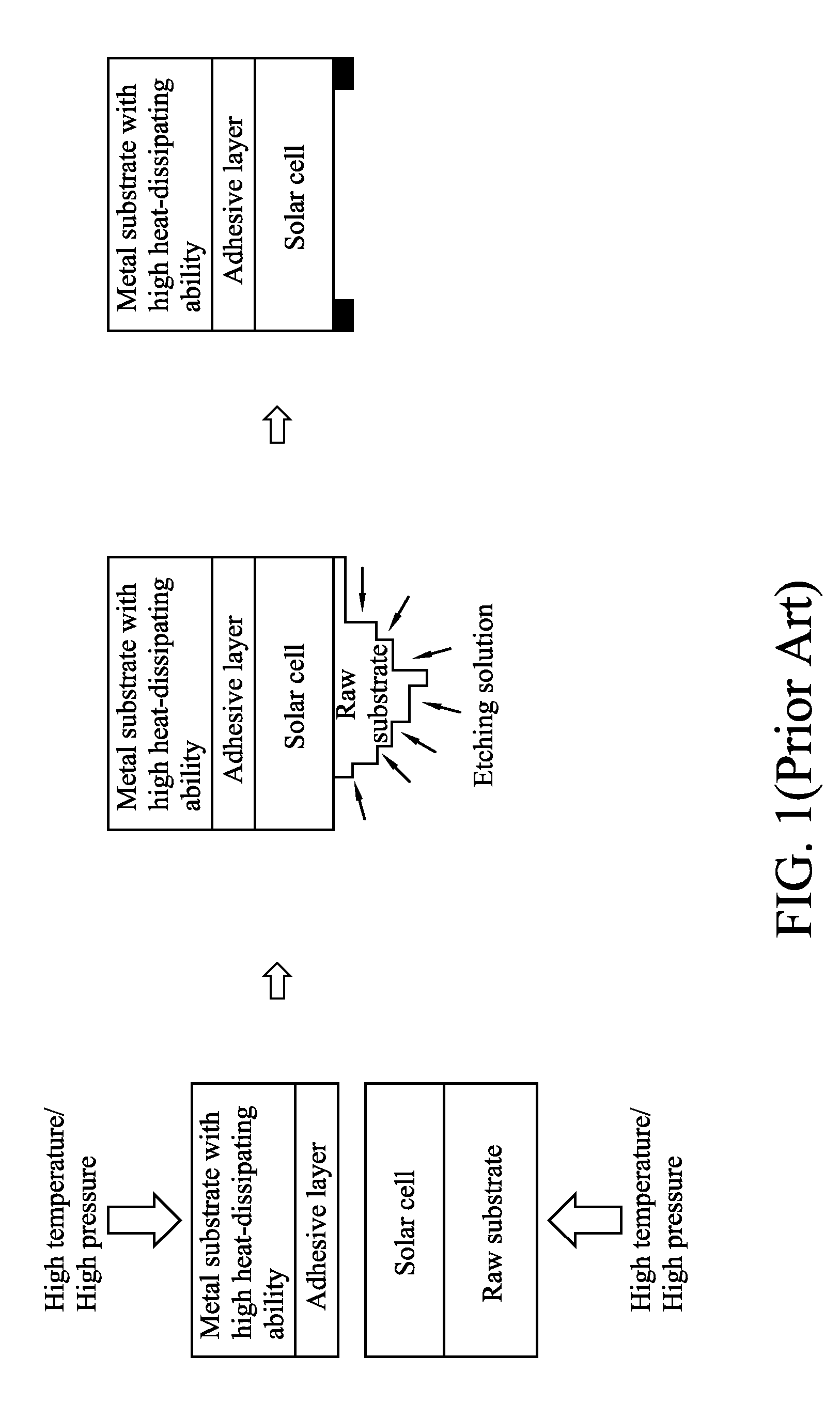
a photoelectric device and lift-off technology, which is applied in the direction of solid-state devices, semiconductor devices, electrical devices, etc., can solve the problems of adverse effects on current-voltage characteristics of solar cells, deterioration of conversion efficiency of solar cells, and inability to recycle and use raw substrates, so as to improve the adverse effect of capillary action

Inactive Publication Date: 2013-11-05
INST NUCLEAR ENERGY RES ROCAEC
View PDF2 Cites 3 Cited by
  • Summary
  • Abstract
  • Description
  • Claims
  • Application Information

AI Technical Summary

Benefits of technology

[0006]In view of the disadvantages of prior art, the object of the present invention is to provide a lift-off structure for substrate of a photoelectric device and the method thereof, by that not only the etching contact area can be increased effectively, but also the adverse effect of capillary action can be improved by the proper etching channel design used in the present invention.

Problems solved by technology

In a condition when a solar cell is operating especially under concentrated-light operation condition, there will be an electric current of several amperes or more flowing through the components inside the solar cell, and consequently, if there is any components inside the solar cell that is designed with poor heat dissipating ability in view of thermal resistance, the temperature of such component as well as the whole solar cell will raise after light shines on the solar cell, causing the conversion efficiency of the solar cell to deteriorate, i.e. the current-voltage characteristics of the solar cell are adversely affected.
As the raw GaAs substrate will be etching away by the chemical solution in the aforesaid conventional solar cell manufacturing process, thus such manufacturing process is disadvantageous in that: first, the raw substrate can not be recycled and used repetitively; and second, the manufacturing cost is increased comparing with those solar cells without the metal substrate with high heat-dissipating ability, owing to the acquisition costs of the raw substrate and the metal substrate with high heat-dissipating ability, and the waste management cost for treating the arsenic-containing waste liquid resulting from the manufacturing process.
However, since such etching of the sacrificial layer can only be performed starting from the lateral of a wafer used for forming solar cells, the lateral etching rate of the sacrificial layer can be very low due to the restriction of capillary action and the limitation relating to a minimum contact area.
Therefore, it can take a very long period of time just for performing a substrate lift-off process upon a large-size wafer.
Thus, such prior-art technique for separating the raw substrate might not be feasible for industrial mass production.

Method used


Image

  • Lift-off structure for substrate of a photoelectric device and the method thereof
  • Lift-off structure for substrate of a photoelectric device and the method thereof
  • Lift-off structure for substrate of a photoelectric device and the method thereof

Examples


first embodiment

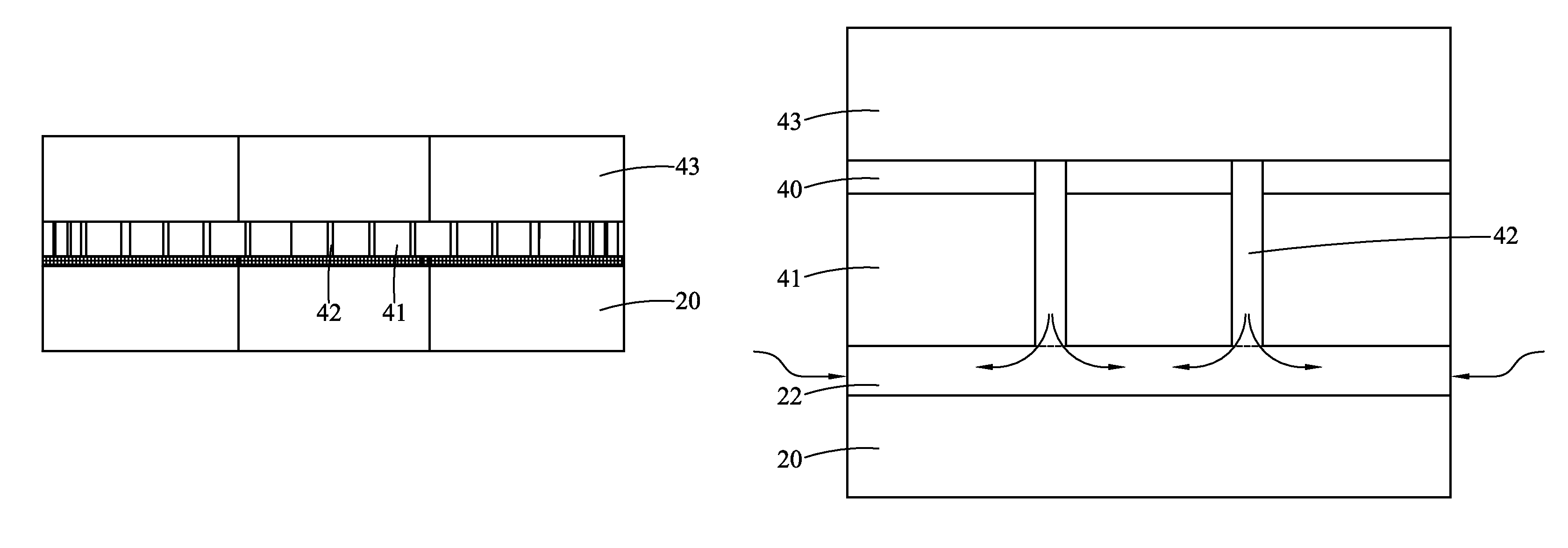
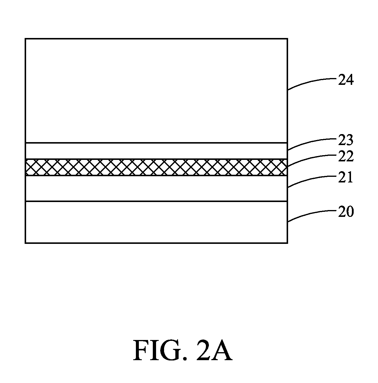
[0041]Please refer to FIG. 2A, which is a schematic diagram showing a lift-off structure for substrate of a photoelectric device according to the invention. In FIG. 2A, the present invention provides a lift-off structure, adapted for a substrate 20 having a photoelectric element 24 formed thereon, which comprises: a buffer layer 21, formed on the substrate 20, and being made of GaAs; an upper sacrificial layer 22, formed on the buffer layer 21, and being made of a material of high aluminum content, such as AlxGa1−xAs, 0.5≦x≦1; an etch stop layer 23, formed on the upper sacrificial layer 22, and being made of a quaternary III-phosphide or ternary III-phosphide, such as GaInP, AlInP, AlGaInP; and the photoelectric element 24, formed on the etch stop layer 23; wherein the substrate 20 can be made of GaAs; and the photoelectric element 24 can substantially be a device selected from the group consisting of: a solar cell, a light-emitting diode, and a p-n junction device.

second embodiment

[0042]Please refer to FIG. 2B, which is a schematic diagram showing a lift-off structure for substrate of a photoelectric device according to the invention. In FIG. 2B, the present invention provides a lift-off structure, adapted for a substrate 20 having a photoelectric element 24 formed thereon, which comprises: a buffer layer 21, formed on the substrate 20, and being made of GaAs; an upper sacrificial layer 22, formed on the buffer layer 21, and being made of a material of high aluminum content, such as AlxGa1−xAs, 0.5≦x≦1; an etch stop layer 23, formed on the upper sacrificial layer 22, and being made of a quaternary III-phosphide or ternary III-phosphide, such as GaInP, AlInP, AlGaInP; a lower sacrificial layer 25, formed on the etch stop layer 23, and being made of a material of high aluminum content, such as AlxGa1−xAs, 0.5≦x≦1; and the photoelectric element 24, formed on the lower sacrificial layer 25, being substantially a device selected from the group consisting of: a sol...

third embodiment

[0043]Please refer to FIG. 2C, which a schematic diagram showing a lift-off structure for substrate of a photoelectric device according to the invention. In FIG. 2C, the present invention provides a lift-off structure, adapted for a substrate 20 having a photoelectric element 24 formed thereon, which comprises: a buffer layer 21, formed on the substrate 20, and being made of GaAs; an etch stop layer 23, formed on the buffer layer 21, and being made of a quaternary III-phosphide or ternary III-phosphide, such as GaInP, AlInP, AlGaInP; a lower sacrificial layer 25, formed on the etch stop layer 23, and being made of a material of high aluminum content, such as AlxGa1−xAs, 0.5≦x≦1; and the photoelectric element 24, formed on the lower sacrificial layer 25; wherein the substrate 20 can be made of GaAs; and the photoelectric element 24 can substantially be a device selected from the group consisting of: a solar cell, a light-emitting diode, and a p-n junction device.

[0044]Please refer to...


PUM


Abstract

The present invention related to a lift-off structure adapted to a substrate having a photoelectric device, the structure comprising: a buffer layer, forming on the substrate; an upper sacrificial layer, forming on the buffer layer; an etch stop layer, forming on the upper sacrificial layer, and the photoelectric device structure forming on the etch stop layer.

Description

FIELD OF THE INVENTION[0001]The present invention relates to a lift-off structure for substrate of a photoelectric device and the method thereof, and more particularly, to a lift-off process adapted for semiconductor and photoelectric industries.BACKGROUND OF THE INVENTION[0002]Generally speaking, under concentrated-light operation condition, III-V multi-junction solar cell can absorb solar energy in a wider wavelength range and as a result its photoelectric conversion efficiency, that is about 43% in laboratory test, is higher than the usual flat-plate solar cell. Hence, the III-V multi-junction solar cells are especially suitable to be applied in large ground-mounted solar power systems for providing electricity in residential sector. Operationally, the electricity output of a solar cell is influenced by the intensity of the light that shines on it while the electricity output of the solar cell can be fed to and used by an external device through its metal electrodes. In a conditi...

Claims


Application Information

Patent Timeline
Patent Type & Authority Patents(United States)
IPC IPC(8): H01L21/30H01L21/46
CPCH01L33/0079H01L31/1896H01L33/0062H01L33/30H01L33/641Y02E10/50H01L33/0093
Inventor TSAI, YU-LIWU, CHIH-HUNGHO, JEI-LIHUANG, CHAO-HUEIYANG, MIN-DE
Owner INST NUCLEAR ENERGY RES ROCAEC
Why Eureka
Try Eureka