Vertical light emitting diodes

a light-emitting diode and vertical technology, applied in the direction of solid-state devices, electric lighting sources, electric light sources, etc., can solve the problems of low extraction efficiency of leds, loss introduced to the trapped waveguide mode, and the existence of optically lossy metal contacts in the close vicinity of light-emitting heterostructure, etc., to achieve low optical loss top contact and low optical loss bottom reflector

Active Publication Date: 2013-11-26
LUMILEDS HLDG BV
View PDF14 Cites 3 Cited by
  • Summary
  • Abstract
  • Description
  • Claims
  • Application Information

AI Technical Summary

Benefits of technology

[0013]The object of the invention is a vertical, flip-chip, light emitting device with a conducting substrate or carrier incorporating a low optical loss bottom reflector and low optical loss top contact.
[0026]In the present invention, conductive multilayer stacks (CMS) are employed to act as low-loss, high-reflectivity regions masking the lossy metal contact regions away from the trapped waveguide modes. These are employed to provide both improved optical light extraction and a vertical conduction path for current spreading in the semiconductor light emitting device.
[0028]Preferably, the top metal contact is deposited on top of another CMR stack to provide for reduced light attenuation from light emitted under the contact region. The finite top contact region contributes to a minimum of around 1% to 5% of the active top surface light emitting region and hence if the light emerging from under these regions can be allowed to escape with minimum loss then an increase in the total luminous output of the LED can be achieved.
[0029]Preferably, the bottom CMR stack and metal contact are roughened to allow for increased scattering and reduced specular reflectivity. This provides an increased probability of trapped light to diffusely reflect and reside in the escape cone of the light emitting material (GaN in this case).
[0030]The use of bottom and top CMR stack layers in the present invention allows the light emitting device to be thinned down to have a total thickness less than 3 μm. This permits the LED to achieve high extraction efficiency while still maintaining high current injection.

Problems solved by technology

However, if light is multiply scattered by the bottom metal reflector then loss is introduced to the trapped waveguide mode.
One of the main limiting factors reducing the extraction efficiency in LEDs is the emitted photons being totally internally reflected and trapped in the high refractive index of the epi-material.
However, one major drawback with such vertical type light emitting structures is the existence of optically lossy metal contacts in the close vicinity of the light emitting heterostructure.
The photons reflected at the interface between the metallic contact surface and the heterostructure material experiences large losses and hence reduces the total light output of the light emitting diode.
However, the single dielectric layer residing between the light emitting region and the lower conductive region hinders good electrical conduction.
In addition, a single dielectric layer will not provide true omni-directional reflectivity and light at angles residing within the escape cone formed between the light emitting medium and the dielectric layer will experience a reflection at the metal contact boundary, which will introduce optical loss.
Additional loss in the light emitting device will also be experienced by the metal electrical contacts at the top surface of the device, which is not desirable.
However, these suffer from several problems such as poor colour gamut, environmental recycling and manufacture issues, thickness and profile, high voltage requirements, poor thermal management, weight and high power consumption.
Conventional High Intensity Discharge (HID) type projector light engines have always been hindered by low efficiency and short lifetime resulting in slow adoption into consumer markets.

Method used


Image

  • Vertical light emitting diodes
  • Vertical light emitting diodes
  • Vertical light emitting diodes

Examples


Embodiment Construction

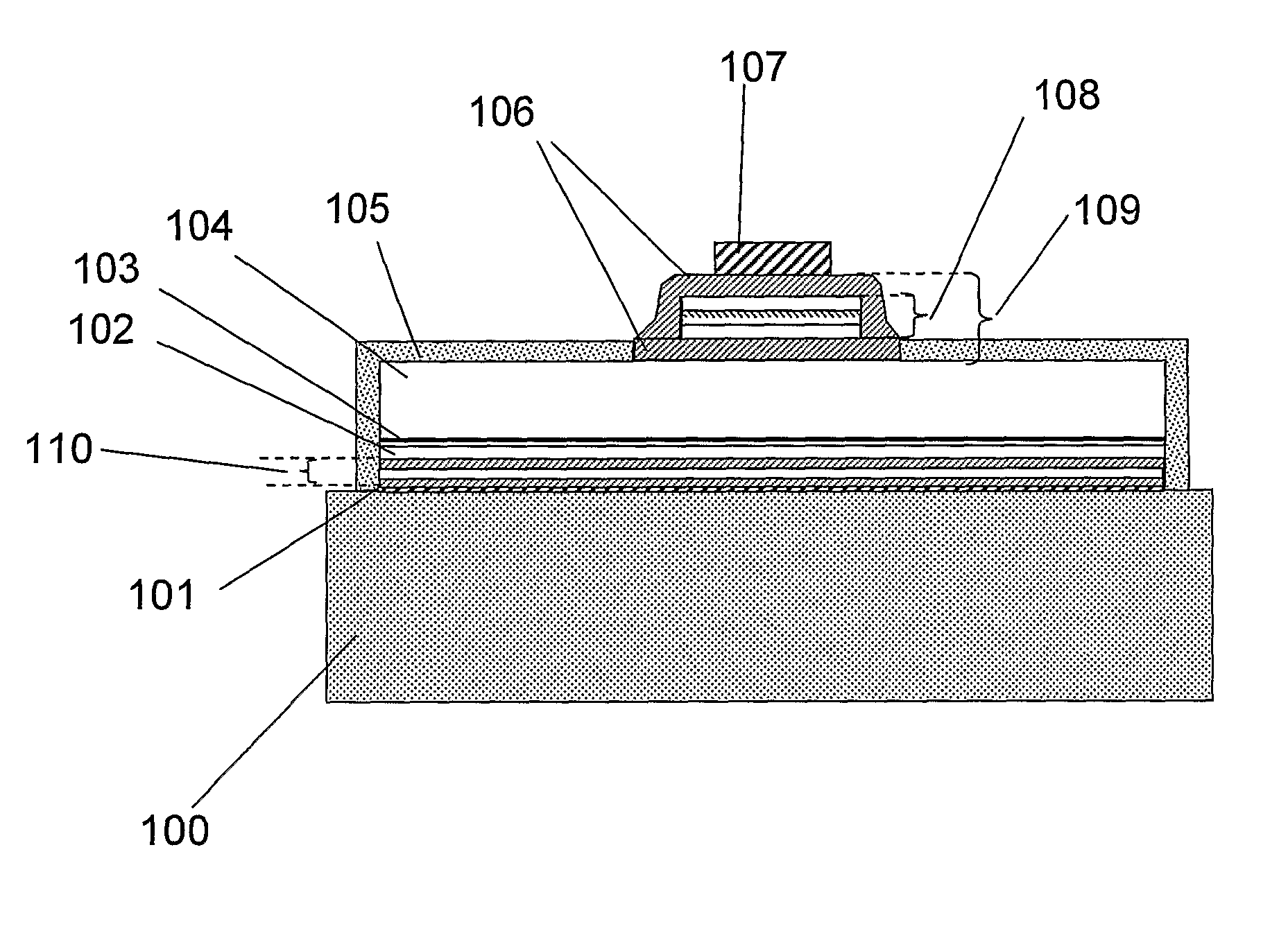
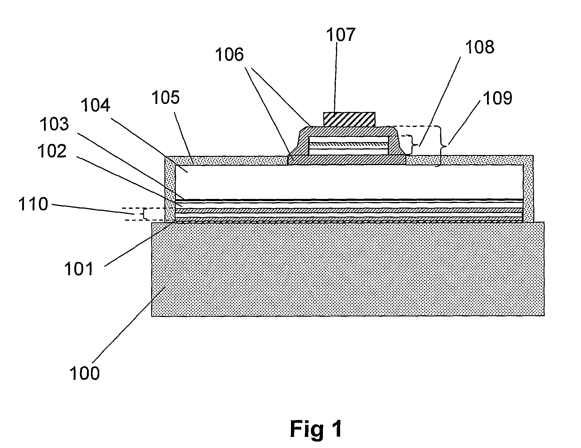
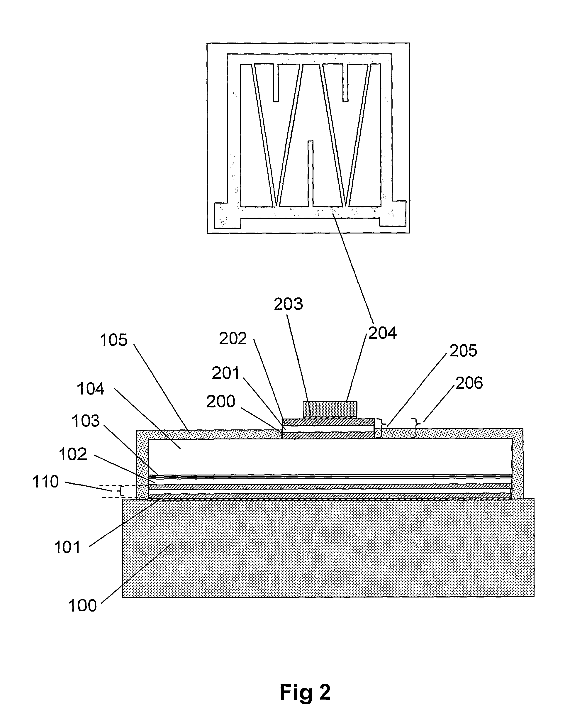
[0059]The present invention provides high wall plug efficiency light emitting devices by improving both the light extraction efficiency as well as the injection efficiency. The invention can be incorporated in a light emitting device of any semiconductor material system such as, but not restricted to, InGaN, InGaP, InGaAs, InP, or ZnO. A GaN based LED having an epitaxial layer formed on a sapphire substrate is used as an example in the present invention.

[0060]GaN light emitting devices comprise a p-n junction heterostructure of refractive index about 2.45. When the light emitting device is forward biased, spontaneously-emitted photons are generated. If the wavevector of the photon resides below the light line (in a frequency-wavevector diagram) of the material, the photon is totally internally reflected and trapped in the high refractive index of the epi-material.

[0061]Table 1 below lists the approximate extraction enhancement achieved using the different techniques commonly employe...


PUM


Abstract

A light emitting device (LED) employs one or more conductive multilayer reflector (CMR) structures. Each CMR is located between the light emitting region and a metal electrical contact region, thereby acting as low-loss, high-reflectivity region that masks the lossy metal contact regions away from the trapped waveguide modes. Improved optical light extraction via an upper surface is thereby achieved and a vertical conduction path is provided for current spreading in the device. In an example vertical, flip-chip type device, a CMR is employed between the metal bottom contact and the p-GaN flip chip layer. A complete light emitting module comprises the LED and encapsulant layers with a phosphor. Also provided is a method of manufacture of the LED and the module.

Description

[0001]This application is a national phase of International Application No. PCT / GB2008 / 000710 filed Mar, 3, 2008, and published in English under WO 2008 / 107654 on Sep. 12, 2008.FIELD OF THE INVENTION[0002]The present invention relates to vertical, flip-chip light emitting devices and particularly to the use of conductive multilayer reflector structures in such devices.BACKGROUND TO THE INVENTION[0003]Vertical light emitting diodes typically employ metal substrates and top contact regions. These characteristically introduce optical loss to trapped waveguide modes residing in the light emitting region. Currently, top surface roughening techniques are employed to extract the maximum amount of light on the first pass of light incident on the top surface. However, if light is multiply scattered by the bottom metal reflector then loss is introduced to the trapped waveguide mode.[0004]Light emitting diodes (LEDs) are based on a forward biased p-n junction. Recently, LEDs have reached high ...

Claims


Application Information

Patent Timeline
Patent Type & Authority Patents(United States)
IPC IPC(8): H01L33/00H01L33/22H01L33/38H01L33/40H01L33/44H05B44/00
CPCH01L33/405H01L33/507H05B33/0857H01L33/0079H01L33/22H01L33/38H01L33/44H01L2924/0002H01L2924/00H01L33/46H01L33/42H05B45/20H01L33/0093H01L33/465
Inventor MCKENZIE, JAMES STUART
Owner LUMILEDS HLDG BV
Why Eureka
Try Eureka