Package configurations for low EMI circuits

a low-emi circuit and configuration technology, applied in the direction of power conversion systems, semiconductor/solid-state device details, semiconductor devices, etc., can solve the problems of reducing and affecting the performance of the circui

Active Publication Date: 2013-11-26
TRANSPHORM INC
View PDF111 Cites 22 Cited by
  • Summary
  • Abstract
  • Description
  • Claims
  • Application Information

AI Technical Summary

Benefits of technology

[0014]In some implementations, the devices described herein can include one or more of the following advantages. Packaged lateral high voltage transistors can reduce or eliminate the capacitance between the drain of the transistor and the circuit or DC ground that can result from the package configuration. Capacitance between the drain of the transistor and the circuit or DC ground can cause current to flow to a ground outside of the desired signal path, which can increase EMI or switching losses during operation of the device. Increased EMI or switching losses can degrade performance of the device or a circuit in which the device is included. Therefore, reducing or eliminating the capacitance between the drain of the transistor and the circuit or DC ground can result in a device or circuit that operates more efficiently. In addition, heat dissipation is improved by some of the transistors described herein. Heat dissipation can improve the longevity and performance of the device. Heat dissipation may also allow for the device to be used in a wider variety of applications.

Problems solved by technology

This again results in a large total capacitance between the drain and the circuit ground.
During operation of the transistor assembly 25, the charging and discharging of capacitor 32 not only causes severe switching losses but also results in the emission of electromagnetic radiation, also known as electromagnetic interference (EMI), thereby degrading the performance of the circuit.
The larger the capacitance of capacitor 32, the higher the switching loss and the intensity of common-mode EMI emission, which results in degradation of electrical performance.

Method used


Image

  • Package configurations for low EMI circuits
  • Package configurations for low EMI circuits
  • Package configurations for low EMI circuits

Examples


Embodiment Construction

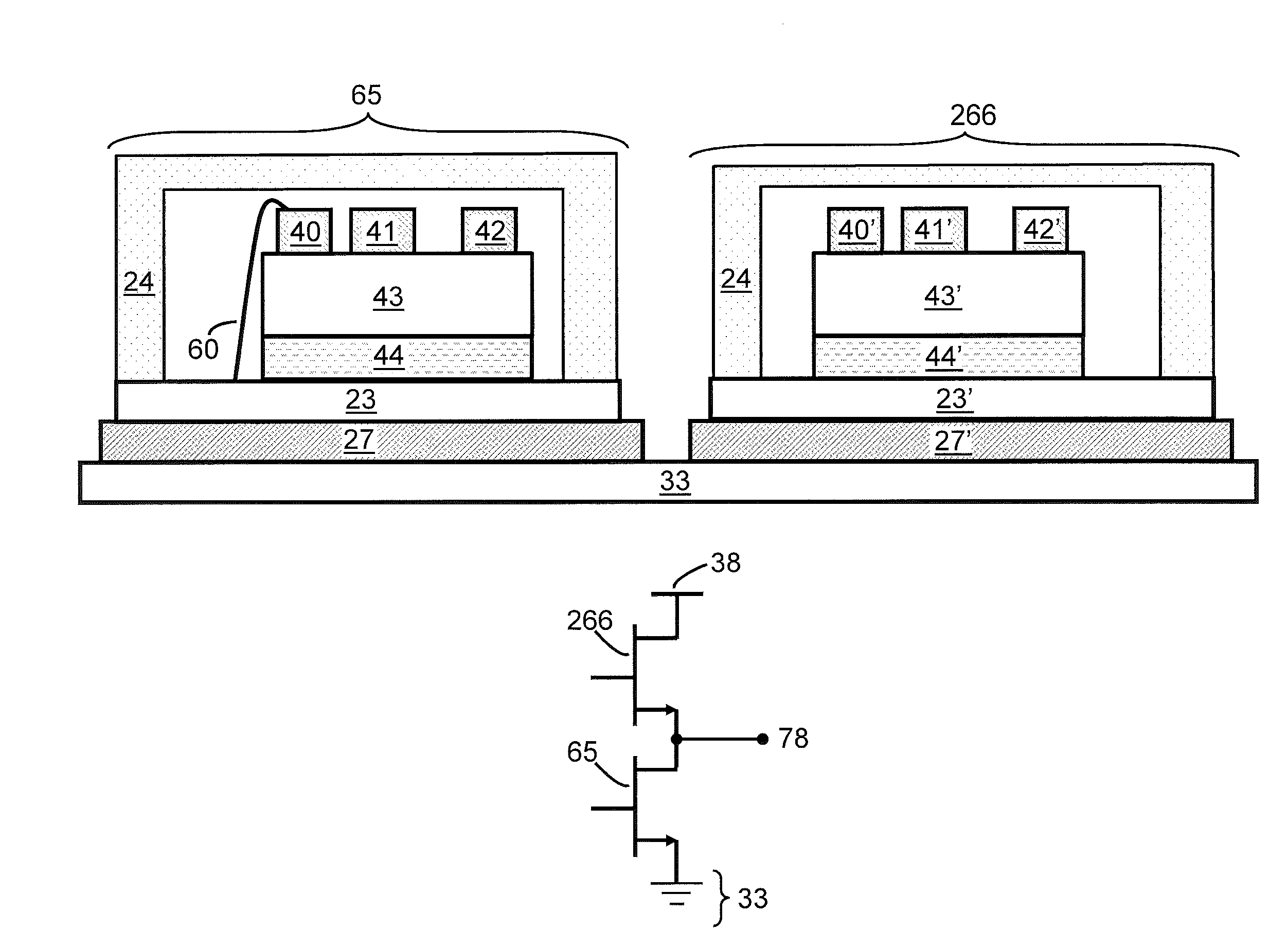
[0028]FIG. 6 is a schematic illustration of an electronic component, which includes a high voltage switching transistor encased in a package. As used herein, a high voltage switching transistor is a transistor optimized for high voltage switching applications. That is, when the transistor is off, it is capable of blocking high voltages, such as about 300V or higher, about 600V or higher, or about 1200V or higher, and when the transistor is on, it has a sufficiently low on-resistance RON for the application in which it is used, i.e., it experiences sufficiently low conduction loss when a substantial current passes through the device. The high voltage switching transistor includes an insulating or semi-insulating portion 44, a semiconductor body 43, a source electrode 40, a gate electrode 41, and a drain electrode 42. In some implementations, the insulating or semi-insulating portion 44 is an insulating or semi-insulating substrate or carrier wafer, while in other implementations, the...


PUM


Abstract

An electronic component includes a high voltage switching transistor encased in a package. The high voltage switching transistor comprises a source electrode, a gate electrode, and a drain electrode all on a first side of the high voltage switching transistor. The source electrode is electrically connected to a conducting structural portion of the package. Assemblies using the abovementioned transistor with another transistor can be formed, where the source of one transistor can be electrically connected to a conducting structural portion of a package containing the transistor and a drain of the second transistor is electrically connected to the second conductive structural portion of a package that houses the second transistor. Alternatively, the source of the second transistor is electrically isolated from its conductive structural portion, and the drain of the second transistor is electrically isolated from its conductive structural portion.

Description

TECHNICAL FIELD[0001]Packaging configurations of semiconductor devices for various circuit applications are described.BACKGROUND[0002]Currently, most high voltage switching circuits are designed using silicon-based transistors, such as Si MOSFETs or IGBTs. A schematic diagram of a Si power MOSFET is shown in FIG. 1. As indicated, the source and gate electrodes 10 and 11, respectively, are on one side of the semiconductor body 13, and the drain electrode 12 is on the opposite side.[0003]Prior to inserting the transistor of FIG. 1 into a discreet circuit, the transistor is encased in a package. Schematic examples of conventional transistor packages are shown in FIGS. 2 and 3. Referring to FIG. 2, the package includes structural portions, such as the case 24 and package base 23, as well as non-structural portions, such as leads 20-22. The case 24 is formed of an insulating material, the package base 23 is formed of a conducting material, the gate lead 21 is formed of a conducting mater...

Claims


Application Information

Patent Timeline
Patent Type & Authority Patents(United States)
IPC IPC(8): H01L23/34H02M1/00
CPCH01L23/057H01L23/36H01L25/115H01L21/77H01L27/0248H01L21/4803H01L21/4814H01L21/4871H01L2224/48091H01L2924/00014H01L2924/13055H01L2924/13091H01L2924/00H01L2924/30107H01L23/481H01L29/772H01L25/072H01L29/2003H01L2224/73265H01L23/3677
Inventor WU, YIFENG
Owner TRANSPHORM INC
Why Eureka
Try Eureka