Method to prepare a stable transparent electrode
a metal electrode, stable technology, applied in the direction of electroluminescent light sources, solid-state diffusion coatings, coatings, etc., can solve the problems of inability to protect the ca layer from oxidation, inability to easily be obtained in large quantities and thus expensive, and incompatibility with some active materials
- Summary
- Abstract
- Description
- Claims
- Application Information
AI Technical Summary
Benefits of technology
Problems solved by technology
Method used
Image
Examples
example 1
Method, Ni-UTMF Obtained and its Characterization
[0043]A 3.4 nanometers thick nickel ultrathin metal film was deposited on a double-side polished BK7 substrate using an ATC ORION 3 HV Sputtering DC System. The sputtering process was performed at room temperature in a pure argon (Ar) atmosphere. Argon pressure was set to 8 mTorr and 200 W DC power electric field was used.
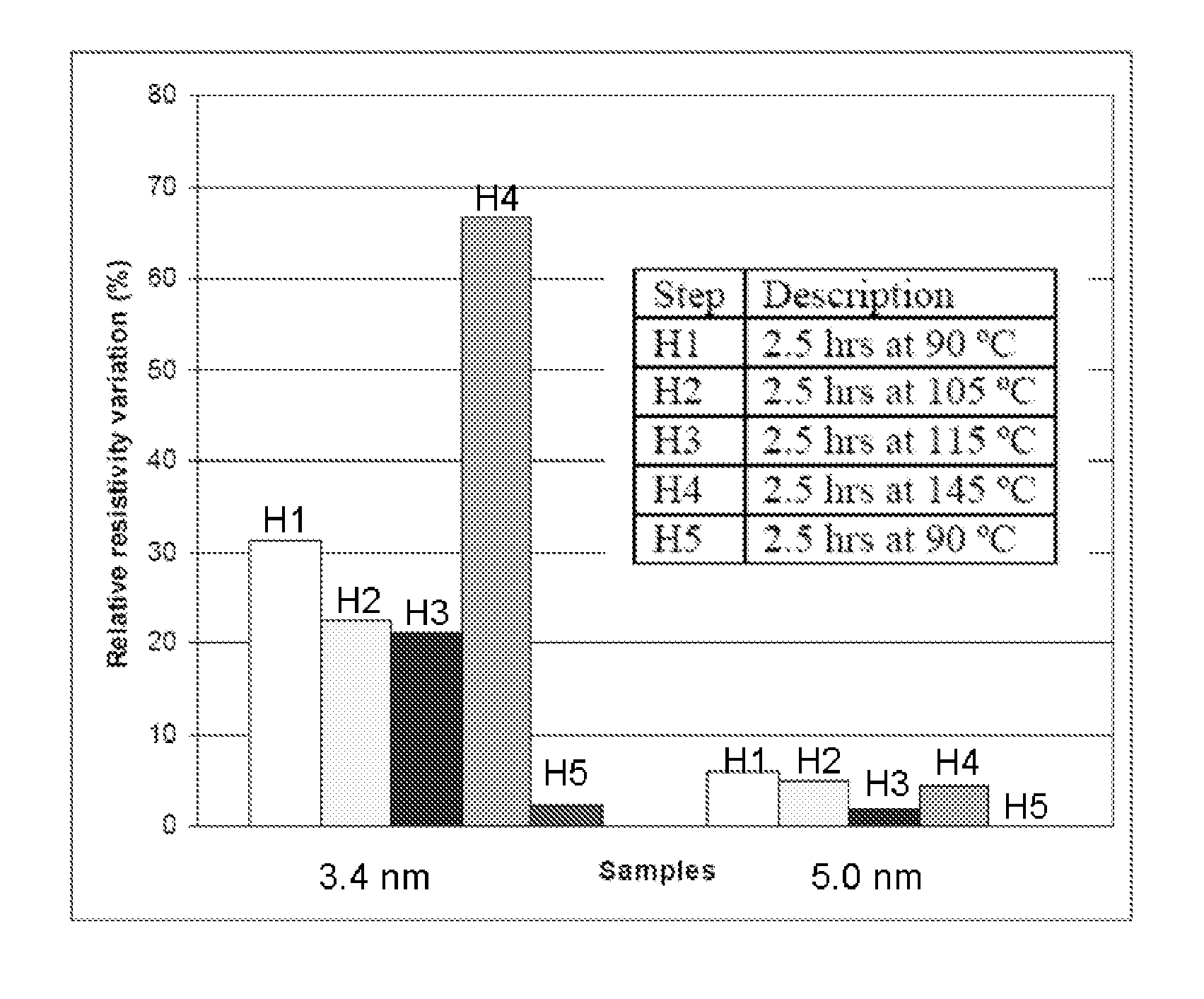
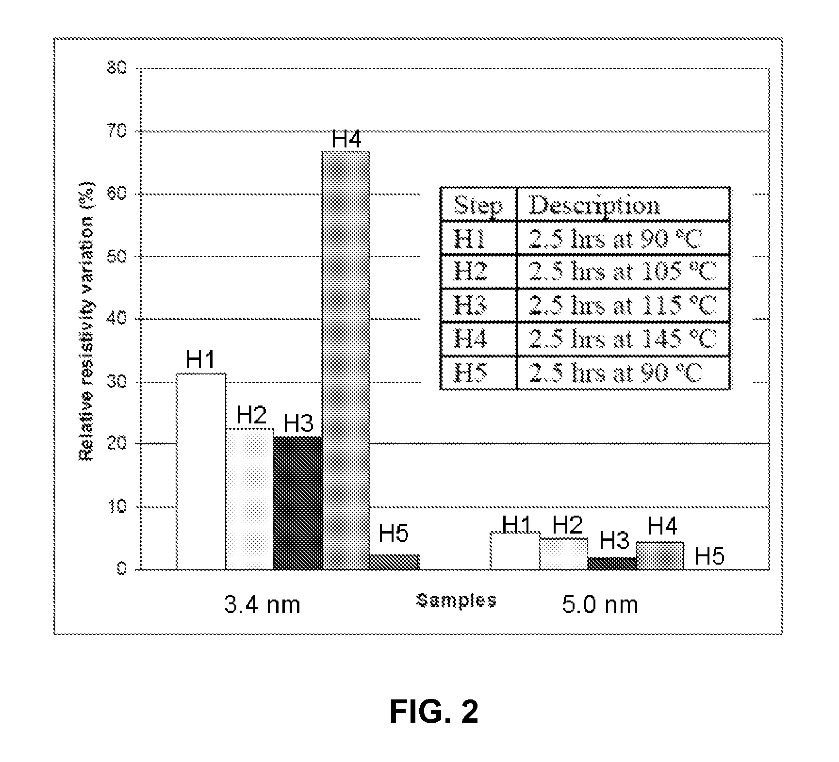
[0044]The electrical resistivity of the film at room temperature was measured straight after deposition and twelve days after the film was deposited, always being kept in ambient atmosphere. A Cascade Microtech 44 / 7S Four Point Probe and a Keithley 2001 multimeter were used for measuring sheet resistance. The sheet resistance (Rs), i.e. the resistance of a square like sheet of layer, is measured in Ω / and is related to the electrical resistivity (ρ) measured in Ω·m through the following relation: Rs=ρ / t with t the thickness of the layer in m. The resistivity of the layer was thus obtained as the ratio between sheet r...
example 2
Method, Ni-UTMF Obtained and its Characterization
[0047]The method of the invention comprised depositing on a substrate a 6 nanometers thick nickel ultrathin metal film. The film was grown on a double-side polished BK7 substrate using an ATC ORION 3 HV Sputtering DC System. The sputtering process was performed at room temperature in a pure argon (Ar) atmosphere. Argon pressure was set to 8 mTorr and 200 W DC power electric field was used.
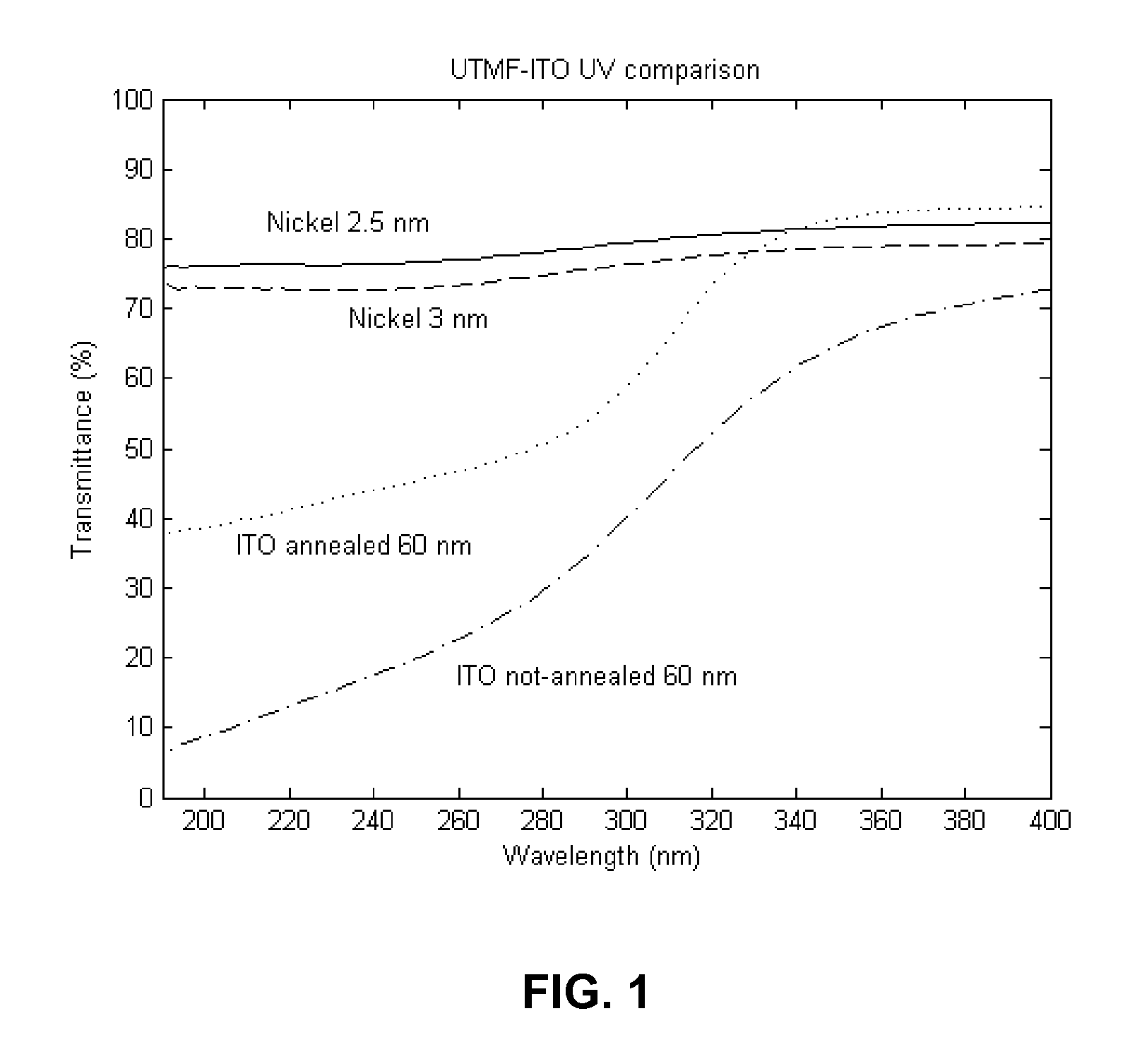
[0048]The electrical resistivity and the optical transmittance of the film are then measured as it is described in the previous example.
[0049]The film undergoes a thermal treatment at about 120° C. and is subjected to a continuous neutral (unionized) oxygen flux of about 20 sccm with kinetic energy of about 130 eV. After about 10 minutes, from electrical resistivity measurements and thickness change measurements, it was found that the formed oxide thickness was about 2.5 nm.
[0050]The Ni-UTMF so obtained was stable.
PUM
| Property | Measurement | Unit |
|---|---|---|
| temperature | aaaaa | aaaaa |
| thick | aaaaa | aaaaa |
| thick | aaaaa | aaaaa |
Abstract
Description
Claims
Application Information


