Optoelectronic device having a sandwich structure and method for forming the same

a technology of optoelectronic devices and sandwich structures, which is applied in the direction of organic semiconductor devices, electroluminescent light sources, electric lighting sources, etc., can solve the problems of increasing the resistance of the device, increasing the cost of producing a large-area device, and increasing the cost of manufacturing a large-area device, so as to improve the performance and reliability of the device, the effect of reducing the manufacturing cos

Active Publication Date: 2014-01-07
NAT TAIWAN UNIV
View PDF10 Cites 4 Cited by
  • Summary
  • Abstract
  • Description
  • Claims
  • Application Information

AI Technical Summary

Benefits of technology

[0010]The object of the present invention is to provide an optoelectronic device and its forming method. The optoelectronic device should reveal excellent performance and the method does not need a high-cost vacuum evaporation deposition and high-temperature annealing step, so that simplifies the manufacturing process, prevents the organic semiconductor layer from being damaged, and decreases the cost.
[0013]According to the optoelectronic devices and method of the present invention, the inorganic semiconductor layers have no need to be formed by the expensive vacuum evaporation process, so that the manufacturing cost can be decreased; meanwhile, the inorganic semiconductor layers have no need to use any annealing process, so that the organic semiconductor layer will not be damaged and the performance and reliability of the device can be promoted.

Problems solved by technology

However, an aluminum electrode, or a buffer layer of calcium or lithium fluoride, is susceptible to being oxidized in the presence of air, causing the resistance of the device to increase.
On the other hand, a buffer layer of PEDOT may over time result in corrosion of the transparent electrode, causing the device to be damaged.
The transition metal oxide layers described above are usually formed by using a vacuum evaporation process, which is costly and difficult for producing a large-area device.
Consequently, the processing temperature is usually higher than the glass transition temperature (Tg) of the organic material, which may result in damage to the organic layer.

Method used


Image

  • Optoelectronic device having a sandwich structure and method for forming the same
  • Optoelectronic device having a sandwich structure and method for forming the same
  • Optoelectronic device having a sandwich structure and method for forming the same

Examples


Embodiment Construction

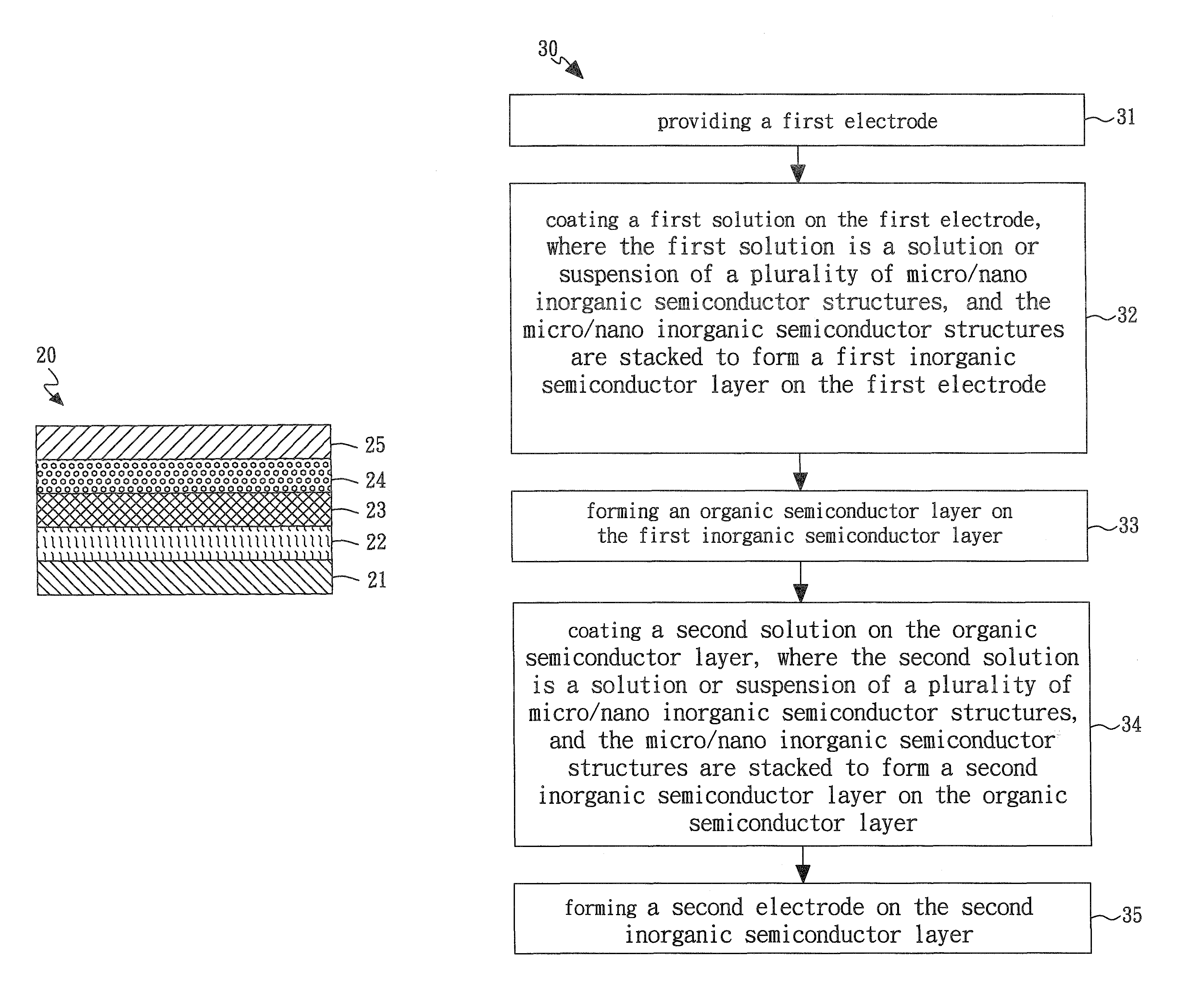
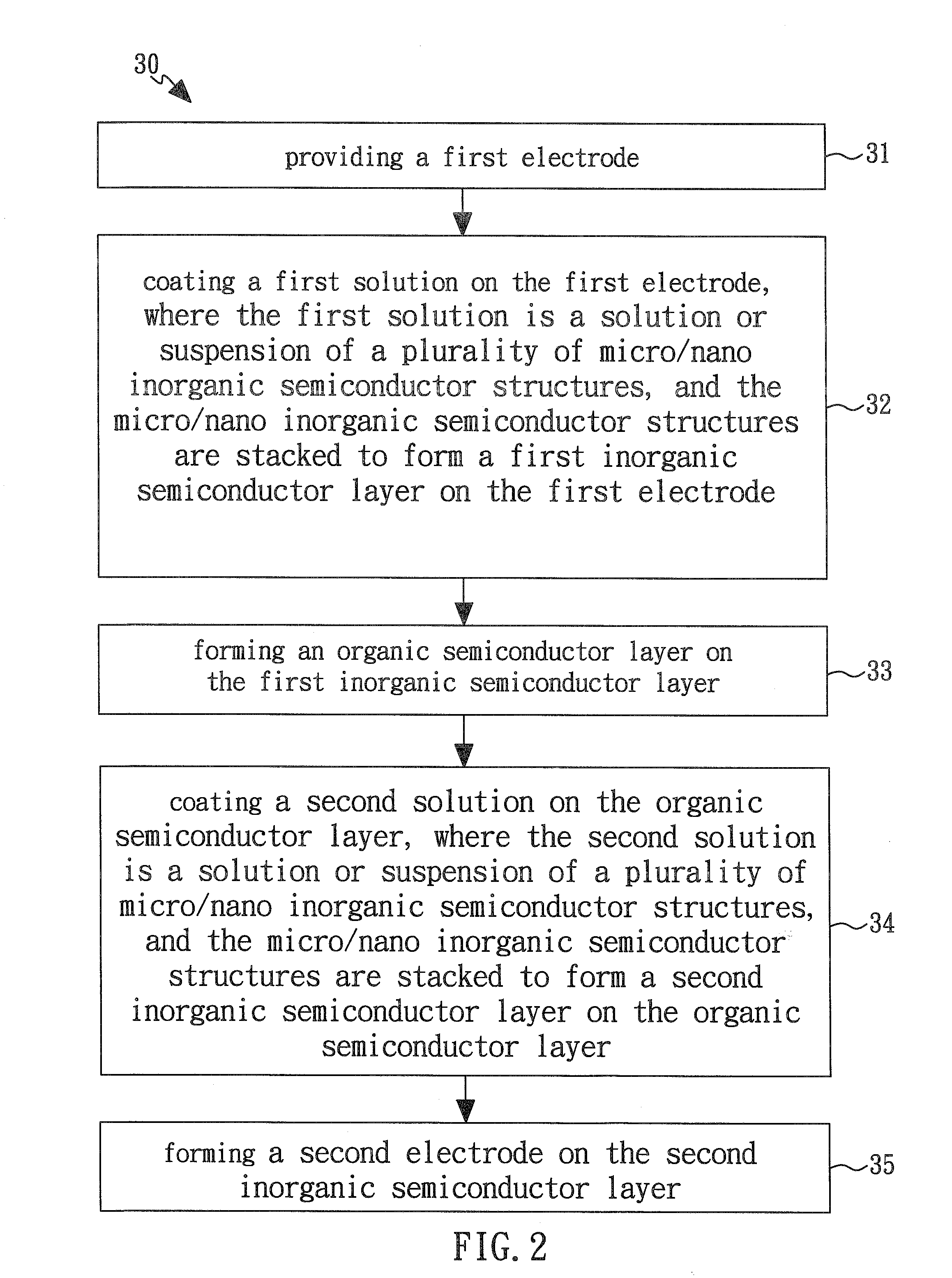
[0018]Reference will now be made in detail to specific embodiments of the invention. Examples of these embodiments are illustrated in the accompanying drawings. While the invention will be described in conjunction with these specific embodiments, it will be understood that it is not intended to limit the invention to these embodiments. On the contrary, it is intended to cover alternatives, modifications, and equivalents as may be included within the spirit and scope of the invention as defined by the appended claims. In the following description, numerous specific details are set forth in order to provide a thorough understanding of the present invention. The present invention may be practiced without some or all of these specific details. In other instances, well-known components and process operations are not described in detail in order not to obscure unnecessarily the present invention. While the drawings are illustrated in detail, it is appreciated that the quantity of the disc...


PUM

PropertyMeasurementUnit
dielectric constantaaaaaaaaaa
concentrationaaaaaaaaaa

Abstract

An optoelectronic device is formed having a sandwich structure, which consists of an inorganic semiconductor layer, an organic semiconductor layer, and another inorganic semiconductor layer, where both of the two inorganic semiconductor layers are produced by a solution process.

Description

CROSS-REFERENCE TO RELATED APPLICATIONS[0001]The entire contents of Taiwan Patent Application No. 098140465, filed on Nov. 27, 2009, from which this application claims priority, are incorporated herein by reference.BACKGROUND OF THE INVENTION[0002]1. Field of the Invention[0003]The present invention generally relates to optoelectronic devices, and more particularly, relates to optoelectronic devices having a sandwich structure and methods for forming the optoelectronic devices.[0004]2. Description of Related Art[0005]Organic optoelectronic devices, such as organic solar cells (OSC), organic light emitting diodes (OLED), organic light sensors, and so on, become increasingly advantageous according to the degree produced in light-weight, small-thickness, large-area, flexible, and low-cost forms.[0006]In order to augment the power conversion efficiency of organic optoelectronic devices, a buffer layer can be disposed between the organic layer and the transparent electrode. For example, ...

Claims


Application Information

Patent Timeline
Patent Type & Authority Patents(United States)
IPC IPC(8): H01L51/40
CPCH01L2251/5369H05B33/12H05B33/10H01L51/5048H10K50/14H10K2102/331
Inventor HUANG, JING-SHUNLIN, CHING-FUH
Owner NAT TAIWAN UNIV
Why Eureka
Try Eureka